


G8 CPCI Enclosure User’s Guide
iii
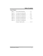
List of Tables
Table 5-1
Environmental Specifications . . . . . . . . . . . . .5-2
Table A1-1
P1 Connector Pin Assignments . . . . . . . . . . .A1-1
Table A1-2
P2 Connector Pin Assignments . . . . . . . . . . .A1-3
Table A1-3
P3 Connector Pin Assignments . . . . . . . . . . .A1-5
Table A1-4
P4 Connector Pin Assignments . . . . . . . . . . .A1-7
Table A1-5
P5 Connector Pin Assignments . . . . . . . . . . .A1-10
Table A1-6
P4 Connector Pin Assignments
(Computer Telephony Bus) . . . . . . . . . . . . . .A1-13
Table of Contents
Summary of Contents for G8
Page 1: ...G8 CPCI Enclosure User s Guide G8 8 Slot CompactPCI Enclosure User s Guide 095 30004 00 Rev A ...
Page 8: ...iv Table of Contents This page was intentionally left blank G8 CPCI Enclosure User s Guide ...
Page 20: ...2 8 G8 CPCI Enclosure User s Guide Chapter 2 Hardware This page was intentionally left blank ...


