Chapter 2. Architecture and technical overview
19
2.2 Processor and cache
The OpenPower 710 server supports one processor module (either a 1-way or 2-way) and
integrated 36 MB L3 cache module.
The storage structure for the POWER5 chip is a distributed memory architecture that
provides high memory bandwidth, although each processor can address all memory and
sees a single shared memory resource. They are interfaced to eight memory slots, controlled
by two SMI-2 controllers, which are located in close physical proximity to the processor
modules. I/O connects to the OpenPower 710 processor module using the GX+ bus. The
processor module provides a single GX+ bus. The GX+ bus provides an interface to I/O
devices through the RIO-2 connections.
The theoretical maximum troughput of the L3 cache is 16-byte read, 16-byte write at a bus
frequency of 825 MHz, which equates to 26400 MB/second or 25.78 GB/s.
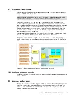
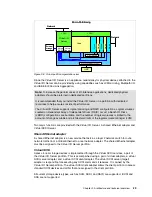
The processor core contains a single processor module and the local memory storage
subsystem for that processor module. Figure 2-3 shows a POWER5 processor core layout
view.
Figure 2-3 POWER5 processor core with DDR1 memory socket layout view
2.2.1 Available processor speeds
At the time of writing, the IBM
Sserver
OpenPower 710 server operates at a processor clock
rate of 1.65 GHz.
2.3 Memory subsystem
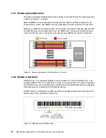
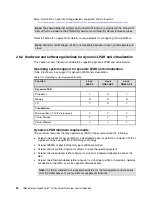
The OpenPower 710 server offers pluggable DIMMs for memory. The system planar provides
eight slots for up to eight pluggable DIMMs. The minimum memory for a OpenPower 710
server is 1 GB and 32 GB as maximum installable memory option. Figure 2-4 shows the
offerings and memory slot availability.
Note: Since the POWER5 processor modules are directly soldered to the system planar,
special care must be taken for sizing and selecting the ideal CPU configuration.
Summary of Contents for 9123710 - eServer OpenPower 710
Page 2: ......
Page 68: ...58 IBM eServer OpenPower 710 Technical Overview and Introduction ...
Page 69: ......


