background image

EM78M611E


Universal Serial Bus Series Microcontroller


Product Specification


(V1.11) 04.20.2007


••••

 11 

(This specification is subject to change without further notice)


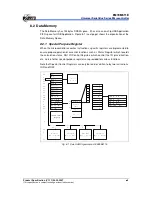
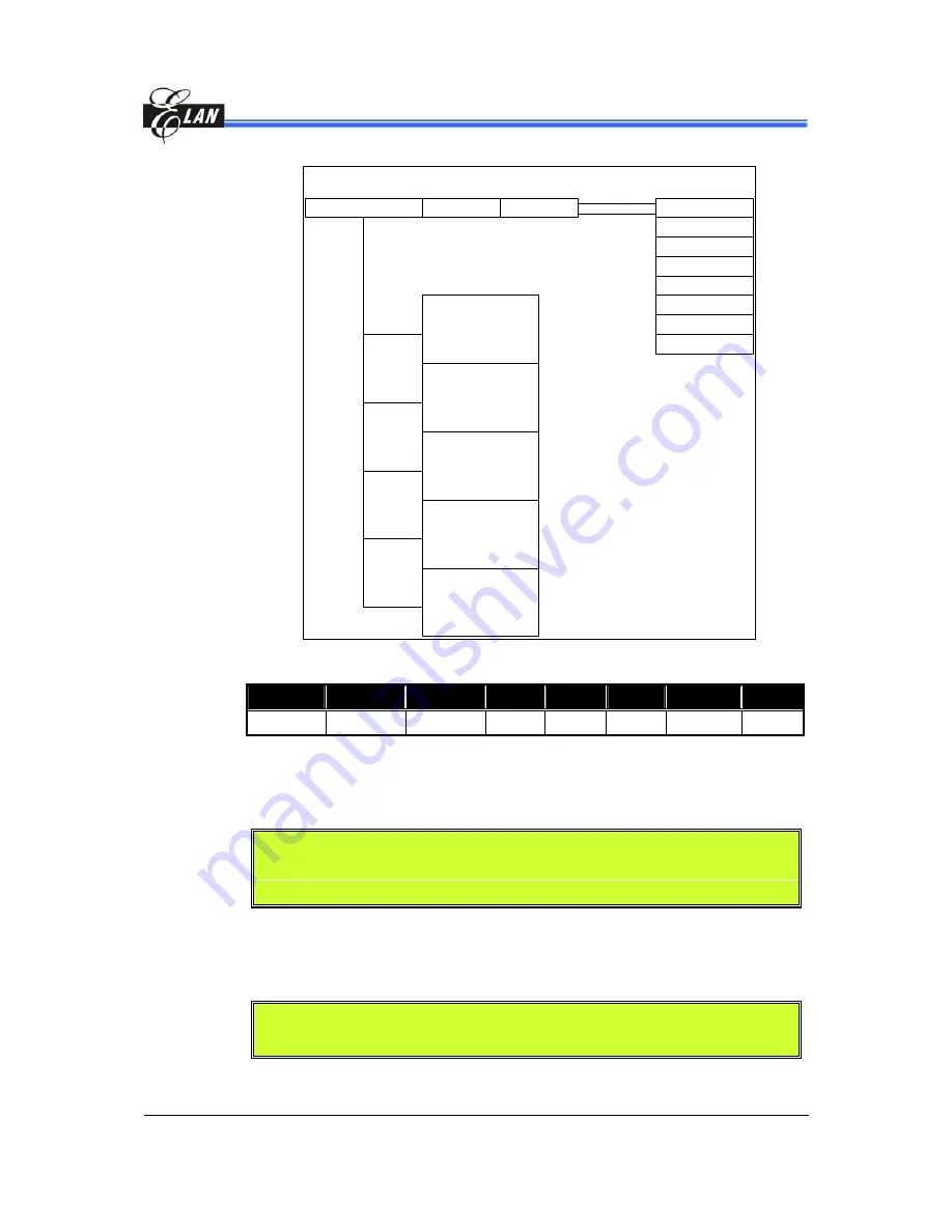
A12  A11  A10

A9  A8

A7~A0

0000

Page 0

03FF
0400

Page 1

07FF
0800

Page 2

0BFF
1000

Page 0

13FF
1400

Page 0

17FF

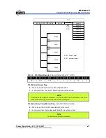
Stack 1
Stack 2
Stack 3
Stack 4
Stack 5
Stack 6
Stack 7
Stack 8

Call

Interrupt

RET

RETL

RETI

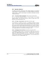
0000 : Reset Vector
0001 : Interrupt Vector


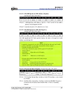
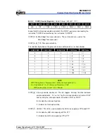
8.2.2.4  R3 (Status Register)  

Default Value:(0B_0001_1XXX) 

Bit 7 

Bit 6 

Bit 5 

Bit 4 

Bit 3 

Bit 2 

Bit 1 

Bit 0 

PS2 

PS1 

PS0 

DC 

R3 [0]  Carry/Borrow Flag 

0

 = No carry-out from the result’s Most Significant bit


1

 = A carry-out from the result’s Most Significant bit occurred 

NOTE 

For  Borrow,  the  polarity  is  reversed.    For  rotate  (RRC,  RLC)  instructions,  this  bit  is 
loaded with either high or low-order bit of the source register. 

R3 [1]  Auxiliary Carry/Borrow Flag

.  For ADD, SUB Instructions  

0

 = No carry-out from the 4th low-order bit of the result


1

 = A carry-out from the 4th low-order bit of the result occurred 

NOTE 

For Borrow, the polarity is reversed. 

Summary of Contents for EM78M611E

Page 1: ...EM78M611E Product Specification DOC VERSION 1 1 ELAN MICROELECTRONICS CORP November 2006...

Page 2: ...ent and may be used or copied only in accordance with the terms of such agreement ELAN Microelectronics products are not intended for use in life support appliances devices or systems Use of ELAN Micr...

Page 3: ...Port 7 I O Register 13 8 2 2 9 R8 Port 8 I O Register 13 8 2 2 10 R9 Port 9 I O Register 13 8 2 2 11 RA EEPROM Control Register 14 8 2 2 12 RB Pattern Detect Application Control Register 14 8 2 2 13...

Page 4: ...on Description 25 8 9 2 Control Register 26 8 9 3 Sampling Rate and Debounce Length 26 8 10 Pulse Width Modulation PWM 28 8 10 1 Function Description 28 8 10 2 Duty Cycle 28 8 10 3 Control Register 28...

Page 5: ...4 bytes of E 2 PROM These series of ICs have many powerful features including Dual clock mode which allows the device to run on low power saving frequency Pattern Detect Application function which is...

Page 6: ...95 and P96 has an internal programmable pull high resistor 25K Each GPIO pin of Port 6 P74 P77 and Port 9 can wake up the MCU from sleep mode by input state change Internal Memory Built in 6K 13 bits...

Page 7: ...mm EM78M611EXAQ 20 pin PDIP 300mil SOP 300mil EM78M611EXBP BM 20 pin SSOP 209mil EM78M611EXDM 24 pin PDIP 600mil SOP 300mil EM78M611EXCP CM 24 pin SSOP 150mil EM78M611EXEM 3 Type Definition The EM78M6...

Page 8: ...2 21 P52 AD2 P53 AD3 P54 AD4 P55 AD5 P56 AD6 P57 AD7 P80 AD8 P81 AD9 P61 AD17 P60 AD16 P87 AD15 P86 AD14 P85 AD13 P84 AD12 P83 AD11 P82 AD10 Fig 3 1 EM78M611EXAP 40 Pin DIP 1 2 3 4 5 6 7 8 9 10 11 12...

Page 9: ...8 P77 P76 VDD OSCI OSCO VSS V3 3 D CLK P74 D DATA P75 P92 SE1 PWM1 P93 SE2 PWM2 P94 VPP VNN P54 AD4 P55 AD5 Fig 3 3 EM78M611EXBP BM DM 20 Pin DIP SOP SSOP 1 2 3 4 5 6 7 8 9 10 11 12 13 14 19 20 21 22...

Page 10: ...bidirectional input output port All pins on this port can be internally pulled high by software control or LED sink pins P94 Vpp I Input only MTP program pin PWM1 PWM2 O PWM output pins D CLK P74 I O...

Page 11: ...ALU ACC R3 Status ROM Instruction Register Instruction Decoder Interrupt Control Reset Sleep Wake up Control 3 3V Regulator USB Device Controller VDD V3 3 Transceiver D D TCC WDT RAM R4 RSR Stack 2 St...

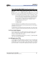
Page 12: ...ds and is divided into six pages Each page is 1K words long After a reset the 13 bit Program Counter PC points to location zero of the program space The Interrupt Vector is at 0x0001 and accommodates...

Page 13: ...ller executes instructions specific registers are implemented to ensure proper operation of essential functions such as Status Register which records the calculation status Port I O Control Registers...

Page 14: ...r Default Value 0B_0000_0000 The TCC register is an 8 bit timer or counter It is readable and writable as any other register The Timer module will be incremented after execution of every instruction c...

Page 15: ...us Register Default Value 0B_0001_1XXX Bit 7 Bit 6 Bit 5 Bit 4 Bit 3 Bit 2 Bit 1 Bit 0 PS2 PS1 PS0 T P Z DC C R3 0 Carry Borrow Flag 0 No carry out from the result s Most Significant bit 1 A carry out...

Page 16: ...l be set to 1 during Power on phase or by WDTC command It is reset to 0 by WDT time out 0 Watchdog timer overflow occurs 1 No Watchdog timer overflow The various states of Power down flag and Time out...

Page 17: ...e 0x0Ch is in the common space Bit 6 and Bit 7 are meaningless 2 R4 10111100 points to the register 0x3C in Bank 2 R4 7 Bk1 R4 6 Bk0 RAM Bank 0 0 1 1 0 1 0 1 Bank 0 Bank 1 Bank 2 Bank 3 8 2 2 6 R5 Por...

Page 18: ...d accessing the FIFO until UDC finishes writing or reading This bit is only readable RC 2 Host Suspend flag If this bit is equal to 1 it indicates that USB bus has no traffic for a specified period of...

Page 19: ...ourth byte of EndPoint Zero user has to use the address of EP0 0x00 and Data Byte Pointer of EP0 0x10 to access it Read the 4th byte of the EP0 FIFO First assign the data byte pointer of EP0 register...

Page 20: ...unction in USB PS2 mode RF 5 6 SE1 SE2 Pattern Detect Interrupt flag These two flags are used for Pattern detect application RF 7 USB Host Resume interrupt flag It will be set only in Dual clock mode...

Page 21: ...aler value and these bits are shown below PSR2 TSR2 PSR1 TSR1 PSR0 TSR0 TCC Rate WDT Rate 0 0 0 1 2 1 1 0 0 1 1 4 1 2 0 1 0 1 8 1 4 0 1 1 1 16 1 8 1 0 0 1 32 1 16 1 0 1 1 64 1 32 1 1 0 1 128 1 64 1 1...

Page 22: ...2 USB IOCA 0 1 These two bits are used to select the operation mode IOCA 1 IOCA 0 Operation Mode 0 0 Detect Mode 0 1 USB Mode 1 0 PS 2 Mode 1 1 USB Test Mode IOCA 2 Pattern Detect Application function...

Page 23: ...ned to wake up the MCU while in Power down mode 0 Enable the function 1 Disable the function IOCB 7 Reserved bit 8 2 3 6 IOCC Port 9 LED Sink Capacity Control Register Default Value 0B_X00X_0000 Bit 7...

Page 24: ...M611E this bit is O K for use IOCE 4 Run bit This bit can be cleared by firmware and set during power on or by the hardware at a falling edge of the wake up signal When this bit is cleared the clock s...

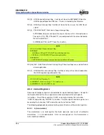
Page 25: ...the ENI instruction will the individual interrupt work After DISI instruction any interrupt will not work even if the respective control bits of IOCF are set to 1 The USB Host Resume Interrupt works o...

Page 26: ...out involving firmware The embedded Series Interface Engine SIE handles the serialization and de serialization of actual USB transmission Thus a developer can concentrate his efforts more in perfectin...

Page 27: ...red c Special registers and Special Control registers are all set to their initial values 8 6 2 Watchdog Reset When the Watchdog timer overflows it causes the Watchdog to reset After it resets the pro...

Page 28: ...me signal is detected on USB Bus 8 8 Interrupt The EM78M611E has one interrupt vector in 0x0001 When an interrupt occurs during an MCU program run it will jump to the interrupt vector 0x0001 and execu...

Page 29: ...bus the status flag RF 2 is set to 1 Its interrupt vector is 0X0001 USB Reset When the UDC detects a USB Reset signal on the USB bus the status flag R 3 is set to 1 Its interrupt vector is 0X0001 USB...

Page 30: ...ce length When a pattern ends the value in the counter is loaded into its respective register and the RB 6 or RB 7 is set to indicate which type of pattern high or low is at its end or which type of p...

Page 31: ...The correlation between the control register value and debounce time are as follows DB 2 DB 1 DB 0 Debounce Time 0 0 0 0 0 0 1 Sampling clock 0 1 0 Sampling clock 2 0 1 1 Sampling clock 3 1 0 0 Sampl...

Page 32: ...The firmware must poll and determine whether the value of these two registers has changed or not 8 10 Pulse Width Modulation PWM 8 10 1 Function Description In PWM mode both PWM1 P 92 and PWM2 P 93 p...

Page 33: ...converter consists of a 5 bit analog multiplexer one Control Register ERA and two data registers RBS RCS for 10 bit resolution The ADC module utilizes successive approximation to convert the unknown...

Page 34: ...P86 0 1 1 1 1 15 P87 1 0 0 0 0 16 P60 1 0 0 0 1 17 P61 1 0 0 1 0 18 P62 1 0 0 1 1 19 P63 1 0 1 0 0 20 P64 1 0 1 0 1 21 P65 1 0 1 1 0 22 P66 1 0 1 1 1 23 P67 ERA 7 AD Converter ready flag 0 1 Start AD...

Page 35: ...3 The stored data of EEPROM are not erased when the power is off and can be read and re written by firmware In some special case of application for example cordless keyboard controller it can store i...

Page 36: ...er Reset detecting high Voltage 3 0 V Ireg 3 3V Regulator driving capacity V3 3 3 3V 100 mA MCU Operation IIL Input Leakage Current for input pins VIN VDD VSS K 1 A VIHX Clock Input High Voltage OSCI...

Page 37: ...ink LED ISink 10 0mA VDD 5V 10 mA IOL4 Output Low Voltage P90 P93 P95 P96 normal mode ISink 10 0mA VREG 3 3V 10 mA IOL5 Output Low Voltage P90 P93 P95 P96 sink LED ISink 10 0mA VREG 3 3V 10 mA RPH1 Pu...

Page 38: ...specification is subject to change without further notice 11 Application Circuit NOTE A BC1 BC2 load Capacitor B C1 bypass capacitor that placed adjacent to VDD pin to minimize noise C C2 C3 power cap...

Page 39: ...addressing mode 0x05 R5 Port 5 P57 P56 P55 P54 P53 P52 P51 P50 0B_0000_0000 0x06 R 6 Port 6 P67 P66 P65 P64 P63 P62 P61 P60 0B_0000_0000 0x07 R 7 Port 7 P77 P76 P75 D DATA P74 D CLK P72 P71 P70 0B_000...

Page 40: ...Register 0B_1111_1111 0x0A IOCA Dual_ Frq 1 Dual_ Frq 0 Remote_ Wake Up ExReg_ Sel PDA PS 2 USB 0B_11x0_0000 0x0B IOCB P96 P95 P94 P93 P92 P91 P90 0B_x111_1111 0x0C IOCC P96 P95 P93 P92 P91 P90 0B_x00...

Page 41: ...ich one of the 64 registers including operation and general purpose registers is to be utilized by the instruction Bits 6 and 7 in R4 determine the selected register bank b Bit field designator that s...

Page 42: ...if zero None 0 0110 00rr rrrr 06rr RRCA R R n A n 1 R 0 C C A 7 C 0 0110 01rr rrrr 06rr RRC R R n R n 1 R 0 C C R 7 C 0 0110 10rr rrrr 06rr RLCA R R n A n 1 R 7 C C A 0 C 0 0110 11rr rrrr 06rr RLC R...

Page 43: ...onic ID_8 ID_7 ID_6 ID_5 ID_4 ID_3 ID_2 ID_1 ID_0 OST_1 OST_0 Frequency Protect Address 001 Bit 5 4 3 2 1 0 Mnemonic AD_Hold R S Package_1 Package_0 Bit 12 11 10 9 8 7 6 Mnemonic QTP_Code1 QTP_Code0 E...

Page 44: ...onnect Resistor Switch Bit 5 AD_Hold Halts the MCU during AD conversion 0 Halts the MCU during AD conversion 1 MCU keeps running during AD conversion Bit 6 EP2_Enable Endpoint 2 Enable 0 Disable 1 Ena...

Reviews: