background image

EM78P312N


8-Bit Microcontroller


12 


Product Specification (V1.0) 10.03.2006


(This specification is subject to change without further notice) 


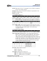
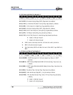
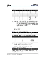
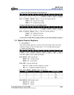
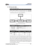
Bank 1 R8 TC2CR/ ADDL (Timer/Counter 2 Control Register, AD Low 2 bits 

Data Buffer) 

Bit 7 

Bit 6 

Bit 5 

Bit 4 

Bit 3 

Bit 2 

Bit 1 

Bit 0 

ADD1 ADD0 

TC2M  TC2S TC2CK2 

TC2CK1 

TC2CK0 

Bit 7 ~ Bit 6 ( ADD1 ~ ADD0 )


:

 AD low 2-bit data buffer 

Bit 4 ( TC2M ) :

 Timer/Counter 2 mode select 

  TC2M = “0” :

 Timer/counter mode 

  TC2M = “1” :

 Window mode 

Bit 3 ( TC2S )


:

 Timer/Counter 2 start control 

  TC2S = “0” :

 Stop and counter clear 

  TC2S = “1” :

 Start 

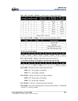
Bit 2 ~ Bit 0 ( TC2CK2 ~ TC2CK0 ) :

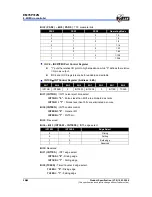
 Timer/Counter 2 Clock Source Select 

TC2CK2 

TC2CK1 

TC2CK0 

Clock Source 

( Normal, Idle ) 

Resolution 

( Fc=8M ) 

Max. Time 

( Fc=8M ) 

0 0 0 

Fc/

2

23

 1.05s 

19.1h 

0 0 1 

Fc/

2

13

 1.02ms 

1.1min 

0 1 0 

Fc/

2

8

 32

μ

s 2.1s 

0 1 1 

Fc/

2

3


1

μ

s 65.5ms 

1 0 0 

Fc 

125ns 7.9ms 

1 0 1 

1 1 0 

External clock (TC2 pin) 


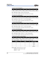
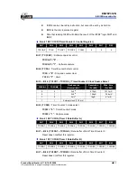
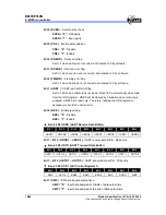
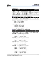
Bank 1 R9 TC2DH (Timer 2 Data Buffer High Byte) 

Bit 7 

Bit 6 

Bit 5 

Bit 4 

Bit 3 

Bit 2 

Bit 1 

Bit 0 

TC2D15 TC2D14 TC2D13 TC2D12 TC2D11 TC2D10  TC2D9  TC2D8 

Bit 7 ~ Bit 0 ( TC2D15 ~ TC2D8 ) :

 16-bit Timer/Counter 2 data buffer high byte.  


Bank 1 RA TC2DL (Timer 2 Data Buffer Low Byte) 

Bit 7 

Bit 6 

Bit 5 

Bit 4 

Bit 3 

Bit 2 

Bit 1 

Bit 0 

TC2D7 TC2D6 TC2D5 TC2D4 TC2D3 TC2D2 TC2D1 TC2D0 

Bit 7 ~ Bit 0 ( TC2D7 ~ TC2D0 ) : 

16-bit Timer/Counter 2 data buffer low byte.  


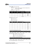
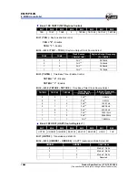
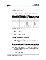
Bank 1 RB ADCR (AD Control Register) 

Bit 7 

Bit 6 

Bit 5 

Bit 4 

Bit 3 

Bit 2 

Bit 1 

Bit 0 

ADREF ADRUN ADCK1  ADCK0  ADP  ADIS2  ADIS1  ADIS0 

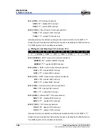
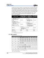
Bit 7 ( ADREF ) :

 AD reference voltage input select. 

 ADREF = “0” :

 Internal VDD, P97 is used as IO.  

 ADREF = “1” :

 External reference pin, P97 is used as reference input pin. 

Summary of Contents for EM78P312N

Page 1: ...EM78P312N 8 BIT Microcontroller Green Product Specification DOC VERSION 1 0 ELAN MICROELECTRONICS CORP October 2006...

Page 2: ...ed or copied only in accordance with the terms of such agreement ELAN Microelectronics products are not intended for use in life support appliances devices or systems Use of ELAN Microelectronics prod...

Page 3: ...ous Receiver Transmitter 28 5 7 1 UART Mode 29 5 7 2 Transmitting 29 5 7 3 Receiving 30 5 7 4 Baud Rate Generator 30 5 8 SPI Serial Peripheral Interface 31 5 8 1 Serial Clock 32 5 8 2 Shift Direction...

Page 4: ...ode Option Register 53 5 17 1 Code Option Register Word 0 53 5 17 2 Customer ID Register 54 5 18 Power on Considerations 54 5 18 1 External Power on Reset Circuit 54 5 18 2 Residue Voltage Protection...

Page 5: ...s inst cycle 3V Peripheral configuration zSerial peripheral interface SPI available zUniversal asynchronous receiver transmitter interface UART available z16 bits Counter Timer TC2 Timer Counter Windo...

Page 6: ...ins P70 can be used as SPI serial clock input output SCK P71 can be used as SPI serial data input SI or UART data receive input RX P72 can be used as SPI serial data output SO or UART data transmit ou...

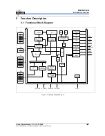
Page 7: ...uction Register ALU PC Interrupt Circuit 8 levelstack 13 bit Interrupt Control Register Oscillation Generation RAM Mux Ext OSC R4 Ext RC Start up Timer WDT TC2 TC3 TC4 UART SPI TCC TBKTC ADC Ain 0 7 S...

Page 8: ...C4D ISFR0 ISFR1 ISFR2 TC3CR TC3DA TC3DB TC2CR ADDL TC2DH TC2DL ADCR ADIC ADDH TBKTC Reserved URC1 URC2 URS URRD URTD Reserved Reserved Reserved Reserved Reserved Reserved SPIC1 SPIC2 SPID Reserved Res...

Page 9: ...hip OTP ROM addresses to the relative programming instruction codes One program page is 1024 words long z R2 is set as all 0 s when under RESET condition z JMP instruction allows direct loading of the...

Page 10: ...curs TCC Overflow External INT1 pin Interrupt Occurs Time Base Timer Interrupt UART Transmit Data Buffer Empty UART Receive Data Buffer Full UART Receive Error TC3 Interrupt SPI Interrupt TC4 Interrup...

Page 11: ...as an 8 bit general purpose read write register See the data memory configuration in Fig 5 2 R5 System Control Register Bit 7 Bit 6 Bit 5 Bit 4 Bit 3 Bit 2 Bit 1 Bit 0 0 0 PS1 PS0 0 1 SIS REM Bits 5...

Page 12: ...I O Data Register Bit 7 Bit 6 Bit 5 Bit 4 Bit 3 Bit 2 Bit 1 Bit 0 0 0 0 0 0 0 P81 P80 Bit 1 Bit 0 P81 P80 Port 81 Port 80 I O data register User can use IOC8 register to define each bit whether input...

Page 13: ...grammable Divider output 1 1 Pulse Width Modulation output RC Timer 4 Data Buffer Bit 7 Bit 6 Bit 5 Bit 4 Bit 3 Bit 2 Bit 1 Bit 0 TC4D7 TC4D6 TC4D5 TC4D4 TC4D3 TC4D2 TC4D1 TC4D0 Bit 7 Bit 0 TC4D7 TC4D...

Page 14: ...eared by software 0 means no interrupt request 1 means with interrupt request z ISFR1 can be cleared by instruction but cannot be set by instruction z IMR1 is the interrupt mask register z Note that r...

Page 15: ...1 Start Bit 5 Bit 4 TC3CK1 TC3CK0 Timer Counter 3 Clock Source Select TC3CK1 TC3CK0 Clock source Normal Idle Resolution Fc 8M Max time Fc 8M 0 0 Fc 2 12 512 S 131 1mS 0 1 Fc 2 10 128 S 32 6mS 1 0 Fc 2...

Page 16: ...0 Fc 2 23 1 05s 19 1h 0 0 1 Fc 2 13 1 02ms 1 1min 0 1 0 Fc 2 8 32 s 2 1s 0 1 1 Fc 2 3 1 s 65 5ms 1 0 0 Fc 125ns 7 9ms 1 0 1 1 1 0 1 1 1 External clock TC2 pin Bank 1 R9 TC2DH Timer 2 Data Buffer High...

Page 17: ...d Bit 3 ADP AD power control ADP 0 Power on ADP 1 Power down Bit 2 Bit 0 ADIS2 ADIS0 Analog Input Pin Select ADIS2 ADIS1 ADIS0 Analog Input Pin 0 0 0 AD0 0 0 1 AD1 0 1 0 AD2 0 1 1 AD3 1 0 0 AD4 1 0 1...

Page 18: ...7 812kHz Bit 3 TBTEN Time Base Timer Enable Control TBTEN 0 Disable TBTEN 1 Enable Bit 2 Bit 0 TBTCK2 TBTCK0 Time Base Timer Clock Source Select TBTCK2 TBTCK1 TBTCK0 Clock Source Normal Idle Interrupt...

Page 19: ...e transmission UTBE bit is read only Therefore writing to the URTD register is necessary when starting transmission shifting Bit 0 TXE Enable transmission TXE 0 Disable TXE 1 Enable Bank 2 R6 URC2 UAR...

Page 20: ...r URBF will be cleared by hardware when receiving is enabled URBF bit is read only Therefore reading the URS register is necessary to avoid an overrun error Bit 0 RXE Enable receiving RXE 0 Disable RX...

Page 21: ...122Kbit s 1 0 1 Fc 2 5 244Kbit s 1 1 0 External clock SCK pin Enable ss pin 1 1 1 External clock SCK pin Disable ss pin Bit 2 EDS Data shift out edge select EDS 0 Rising edge EDS 1 Falling edge Bit 1...

Page 22: ...4 Bit 3 Bit 2 Bit 1 Bit 0 SPID7 SPID6 SPID5 SPID4 SPID3 SPID2 SPID1 SPID0 Bit 7 Bit 0 SPID7 SPID0 SPI data buffer Bank 3 RA PHC1 Pull High Control Register 1 Bit 7 Bit 6 Bit 5 Bit 4 Bit 3 Bit 2 Bit 1...

Page 23: ...low R10 R1F and R20 R3F including Banks 0 3 are General Purpose Register 5 3 Special Purpose Registers A Accumulator Internal data transfer operation or instruction operand holding usually involves t...

Page 24: ...ritable INTCR INT Control Register Address 0Bh Bit 7 Bit 6 Bit 5 Bit 4 Bit 3 Bit 2 Bit 1 Bit 0 INT1NR INT0EN 0 INT3ES1 INT3ES0 0 INT1ES TC2ES Bit 7 INT1NR INT1 noise reject time select INT1NR 0 Pulses...

Page 25: ...Calibration Bit 6 SIGN Offset voltage Polarity bit SIGN 0 Negative voltage SIGN 1 Positive voltage Bit 5 Bit 3 VOF 2 VOF 0 Offset voltage bits IMR1 Interrupt Mask Register 1 Address 0Eh Bit 7 Bit 6 B...

Page 26: ...0 TCIE0 Bit 6 UERRIE UART receive error interrupt enable bit UERRIE 0 disable UERRIF interrupt UERRIE 1 enable UERRIF interrupt Bit 5 URIE UART receive mode interrupt enable bit URIE 0 disable RBFF in...

Page 27: ...ormal SLEEP pin wake up Normal Idle Set SIS 0 execute SLEP instruction Idle Normal Interrupt Table 3 Operation Mode Operation Mode Frequency CPU Code On chip Peripherals Reset Reset Reset Normal Fosc...

Page 28: ...No effect 1 Individual interrupt source in IMR1 IMR2 2 WDT interrupt request 3 INT0 4 Execute ENI instruction No effect 1 Wake up 2 Jump to an Interrupt vector after RETI instruction then jump to the...

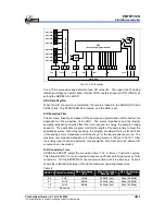
Page 29: ...e ADC The source impedance and the internal sampling impedance directly affect the time required to charge the sample holding capacitor The application program controls the length of the sample time t...

Page 30: ...R W R W 0 UERRIF RBFF TBEF TBIF EXIF1 0 TCIF0 Bank 0 0x0F ISFR2 0 R W R W R W R W R W 0 R W 0 UERRIE URIE UTIE TBIE EXIE1 0 TCIE0 SPR 0x0F IMR2 0 R W R W R W R W R W 0 R W MUX Fosc 2 Fosc 2 Fosc 2 Fo...

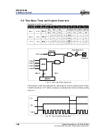
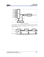
Page 31: ...sc 2 Fosc 2 23 21 16 14 13 12 11 9 TBKTC TBTCK2 0 3 Falling Edge Detector TBT Interrupt TBTEN Fig 5 8 TBT Configuration The Time Base Timer is used to generate the base time for key scan or dynamic di...

Page 32: ...URTD 6 URTD 5 URTD 4 URTD 3 URTD 2 URTD 1 URTD0 Bank 2 0X09 URTD W W W W W W W W 0 UERRIF RBFF TBEF TBIF EXIF1 0 TCIF0 Bank 0 0x0F ISFR2 R W R W R W R W R W R W 0 UERRIE URIE UTIE TBIE EXIE1 0 TCIE0...

Page 33: ...e samples it is recognized as normal start bit and the receiving operation is started START bit D0 D1 D2 Dn Parity bit STOP bit 1 bit 7 or 8 bits One character or frame 1 bit 1 bits Idle state mark I...

Page 34: ...p bit are received After one character received the UART generates a RBFF interrupt if enable And URBF bit of URS register will be set to 1 4 The UART makes the following checks a Parity check The num...

Page 35: ...5 TCIF2 ADIF 0 EXIF3 TCIF4 SPIF TCIF3 Bank 0 0x0E ISFR1 R W R W R W R W R W R W R W EXIE5 TCIE2 ADIE 0 EXIE3 TCIE4 SPIE TCIE3 SFR 0x0E IMR1 R W R W R W R W R W R W R W SHIFT Register SPID reg Prescale...

Page 36: ...r at the end of the data output time 5 8 3 Transfer Mode The transmit receive transmit receive mode can be selected by setting SPIM0 SPIM1 a 8 bit Transmit Mode Set SPIM0 SPIM12 to transmit mode and w...

Page 37: ...in a0 a1 a2 a3 a4 a5 a6 a7 a SPID b0 b1 b2 b3 b4 b5 b6 b7 read data b shift finish Fig 5 15 Receive Mode 8 bit 1 word c 8 bit Transmit Receive Mode Set SPIM0 SPIM1 to transmit receive mode and write d...

Page 38: ...eive Mode 8 bit 1 word d Multiple Device Connect SS When selecting external clock for transfer clock source the SS function can be used This pin SS will be active when the SS function is enabled else...

Page 39: ...TC2D8 Bank 1 0X09 TC2DH R W R W R W R W R W R W R W R W TC2D7 TC2D6 TC2D5 TC2D4 TC2D3 TC2D2 TC2D1 TC2D0 Bank 1 0X0A TC2DL R W R W R W R W R W R W R W R W EXIF5 TCIF2 ADIF 0 EXIF3 TCIF4 SPIF TCIF3 Ban...

Page 40: ...TC2 pin and either rising or falling can be selected by setting TC2ES When the contents of the up counter matched with the TCR2 TCR2H TCR2L then interrupt is generated and the counter is cleared Coun...

Page 41: ...t 4 Bit 3 Bit 2 Bit 1 Bit 0 TC3CAP TC3S TC3CK1 TC3CK0 TC3M 0 0 0 Bank 1 0X05 TC3CR R W R W R W R W R W TC3DA7 TC3DA6 TC3DA5 TC3DA4 TC3DA3 TC3DA2 TC3DA1 TC3DA0 Bank 1 0X06 TC3DA R W R W R W R W R W R W...

Page 42: ...e In Counter mode counting up is performed using the external clock input pin TC3 pin and either rising or falling edge can be selected by INT3ES0 but both edge cannot be used When the contents of the...

Page 43: ...capture and overflow detection are halted until TCR3DA is read out K 2 K 1 K 0 1 m 1 m m 1 n 1 n 0 1 2 3 FE FF0 1 2 3 Source Clock Up counter TC3 Pin Input TCR3DA TCR3DB TC3 Interrupt Reading TCR3DA K...

Page 44: ...med on the rising edge of the external clock input pin TC4 pin When the contents of the up counter matched with the TCR4 then interrupt is generated and the counter is cleared Counting up resumes afte...

Page 45: ...R4 TC4 Interrupt n n n 2 F F PWM Match Overflow n 1 n Match n 2 Overflow 1 Period n m m m Overwrite Shift m 1 1 m Fig 5 26 Timing Chart for PWM Mode 5 12 TCC WDT Prescaler An 8 bit counter is availabl...

Page 46: ...M U X IOD PCRD Fig 5 27 The I O Port and I O Control Register Circuit 5 14 Reset and Wake up 5 14 1 Reset A reset is initiated by one of the following events 1 Power on reset 2 RESET pin input low 3 W...

Page 47: ...in The controller will be waken up and execute the next instruction after entering Sleep mode All the registers will maintain their original values before SLEP instruction was executed 2 RESET pin pul...

Page 48: ...DT time out 0 P P P P U U U 0x0C ADOSC R Wake up from Sleep Idle mode 0 P P P P U U U Bit Name EXIE5 TCIE2 ADIE X EXIE3 TCIE4 SPIE TCIE3 Power on 0 0 0 U 0 0 0 0 RESET and WDT time out 0 0 0 U 0 0 0 0...

Page 49: ...U U U P P Bit Name P97 P96 P95 P94 P93 P92 P91 P90 Power on 1 1 1 1 1 1 1 1 RESET and WDT time out 1 1 1 1 1 1 1 1 0x09 Port 9 Wake Up from Sleep Idle mode P P P P P P P P Bit Name TC4FF1 TC4FF0 TC4S...

Page 50: ...DDL Wake up from Sleep Idle mode P P U P 0 P P P Bit Name TC2D15 TC2D14 TC2D13 TC2D12 TC2D11 TC2D10 TC2D9 TC2D8 Power On 0 0 0 0 0 0 0 0 RESET and WDT time out 0 0 0 0 0 0 0 0 0x09 TC2DH Wake up from...

Page 51: ...P P P P P P P P Register Bank 3 Address Name Reset Type Bit 7 Bit 6 Bit 5 Bit 4 Bit 3 Bit 2 Bit 1 Bit 0 Bit Name SMP DCOL BRS2 BRS1 BRS0 EDS DORD WBE Power on 0 0 0 0 0 0 0 0 RESET and WDT time out P...

Page 52: ...nd P of the Status Register The values of T and P are used to verify the event that triggered the processor to wake up Table 7 shows the events that may affect the status of T and P Table 7 The Values...

Page 53: ...1 TBEF 0015 6 Internal UART Receive ENI URIE 1 TBFF 0018 7 Internal UART Receive error ENI UERRIE 1 UERRIF 001B 8 Internal TC3 ENI TCIE3 1 TCIF3 0021 9 Internal SPI ENI SPIE 1 SPIF 0024 10 Internal TC...

Page 54: ...frequencies of the crystal resonator under different VDDs is listed below Table 10 Oscillator Modes Defined by SDCS and OSC Mode OSC Oscillator 1 High frequency oscillator Single Clock 0 ERC Table 11...

Page 55: ...809N Fig 5 30 Crystal Resonator Circuit Table12 Capacitor Selection Guide for Crystal Oscillator or Ceramic Resonator Oscillator Type Frequency Mode Frequency C1 pF C2 pF 2 0 MHz 20 40 20 40 Ceramic R...

Page 56: ...ries slightly from one chip to another due to the manufacturing process variation In order to maintain a stable system frequency the values of the Cext should not be less than 20pF and the value of Re...

Page 57: ...Code Option Register The EM78P312N has one CODE option word that is not part of the normal program memory The option bits cannot be accessed during normal program execution Code Option Register and C...

Page 58: ...oltage Detector POVD with a detecting level of 2 1V It will work well if VDD rises fast enough 10 ms or less In many critical applications however additional components are required to provide solutio...

Page 59: ...replaced device power VDD is taken off but residue voltage remains The residue voltage may trip below VDD minimum but not to zero This condition may cause a poor power on reset Fig 35 and Fig 36 show...

Page 60: ...K is low and four oscillator clocks if CLK is high Note that once the 4 oscillator periods within one instruction cycle is selected as in Case A the internal clock source to TCC should be CLK Fosc 4 n...

Page 61: ...R 1 A skip if zero None 0 0101 11rr rrrr 05rr DJZ R R 1 R skip if zero None 0 0110 00rr rrrr 06rr RRCA R R n A n 1 R 0 C C A 7 C 0 0110 01rr rrrr 06rr RRC R R n R n 1 R 0 C C R 7 C 0 0110 10rr rrrr 0...

Page 62: ...Rating Temperature under bias 40 C to 85 C Storage temperature 65 C to 150 C Input voltage 0 3V to 6 0V Output voltage 0 3V to 6 0V Operating Frequency 2clk DC to 10MHz 6 2 Recommended Operating Condi...

Page 63: ...hreshold Voltage Schmitt Trigger RESET TCC INT 0 7 VDD VDD 0 3V V VILT1 Input Low Threshold Voltage Schmitt Trigger RESET TCC INT 0 3V 0 3 VDD V VIHX1 Clock Input High Voltage OSCI in crystal mode 0 7...

Page 64: ...ESET TCC 0 7 VDD VDD 0 3V V VILT2 Input Low Threshold Voltage Schmitt Trigger RESET TCC 0 3V 0 3 VDD V VIHX1 Clock Input High Voltage LOSCI OSCI in crystal mode 0 7 VDD VDD 0 3V V VILX1 Clock Input Lo...

Page 65: ...rent VDD VAREF 5 0V VASS 0 0V V reference from VREF 200 250 300 A RN Resolution VDD VAREF 5 0V VASS 0 0V 9 10 Bits LN Linearity error VDD 2 5 to 5 5V Ta 25 C 0 1 2 LSB DNL Differential nonlinear error...

Page 66: ...2000 ns Twdt Watchdog timer period Ta 25 C 11 3 16 2 21 6 ms Tset Input pin setup time 0 ns Thold Input pin hold time 20 ns Tdelay Output pin delay time Cload 20pF 50 ns Tstup1 SDI data setup time Se...

Page 67: ...tice 7 3 Timing Diagram RESET Timing CLK 0 CLK RESET NOP Instruction 1 Executed Tdrh TCC Input Timing CLKS 0 CLK TCC Ttcc Tins AC Testing Input is driven at 2 4V for logic 1 and 0 4V for logic 0 Timin...

Page 68: ...EM78P312NAK SDIP 28 300 mil EM78P312NM SOP 28 300 mil EM78P312NS SSOP 28 209 mil Y S J Green product does not contain hazardous substances The third edition of Sony SS 00259 standard Pb content shoul...

Reviews: