background image

INSTALLATIONS


24


MB860 User’s Manual


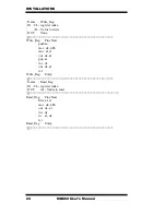
; Name  : Write_Reg 
; IN  : CL - register index 

  AL - Value to write 

; OUT 

: None 

;[]================================================ 
Write_Reg 

Proc Near 


push ax 


mov  dx, 4Eh 


mov  al,cl 


out  dx,al 


pop  ax 


inc  dx 


out  dx,al 


ret 

Write_Reg 

Endp 

;[]================================================ 
; Name  : Read_Reg 
; IN  : CL - register index 
; OUT 

: AL - Value to read 

;[]=================================================== 
Read_Reg 

Proc Near 


Mov al, cl 


mov  dx, 4Eh 


out  dx, al 


inc  dx 


in  al, dx 


ret 

Read_Reg 

Endp 

;[]================================================ 


Summary of Contents for MB860

Page 1: ...MB860 Transmeta Efficeon Mini ITX Motherboard USER S MANUAL Version 1 0 ...

Page 2: ...ational Business Machines Corporation Transmeta Crusoe Code Morphing and LongRun are trademarks of Transmeta Corporation Microsoft Windows is a registered trademark of Microsoft Corporation Winbond is a registered trademark of Winbond Electronics Corporation All other product names or trademarks are properties of their respective owners ...

Page 3: ... on MB860 11 Watchdog Timer Configuration 21 Digital I O Sample Code 25 BIOS Setup 28 Drivers Installation 50 ALi Integrated Driver Installation 51 Transmeta TM8000 AGP Driver Installation 53 Analog Device AC 97 Audio Driver Installation 56 ATI Mobility Radeon M7 M9 VGA Driver Installation 57 Realtek LAN Drivers Installation 58 Appendix 60 A I O Port Address Map 60 B Interrupt Request Lines IRQ 61...

Page 4: ...iv MB860 User s Manual This page is intentionally left blank ...

Page 5: ...es with four serial ports and four USB ports support watchdog timer and one PCI slot for added functionality and expandability About the processor features Enhanced LongRun Power Management Unlike conventional x86 processors Transmeta s Enhanced LongRun power management technology is part of the Efficeon processor s Code Morphing Software This combination allows the Efficeon processor to seamlessl...

Page 6: ...ist Your MB860 package should include the items listed below The MB860 Mini ITX motherboard This User s Manual 1 CD containing chipset drivers and flash memory utility Optional cables such as 2 IDE ribbon cables 40 pin 44 pin 3 COM port cables ...

Page 7: ...or RTL8110s 32 Gigabit Ethernet controllers Audio Built in ALI M1563M sound controller AC97 Codec ADI AD1885 Line out Line in Mic Memory type 1 x DDR 2 5V 266 333 DDR SDRAM SO DIMM Module Max 1GMB LPC I O Winbond W83627 IrDA LPT COM1 2 FDC 2 Keyboard Mouse Controller COM1 RS232 COM2 RS232 RTC CMOS Built in ALI 1563M Secondary LPC I O Fintek F81216 Support COM3 COM4 RS232 Battery Lithium battery Lo...

Page 8: ...INTRODUCTION 4 MB860 User s Manual Board Dimensions ...

Page 9: ... provides information on how to use the jumpers and connectors on the MB860 in order to set up a workable system The topics covered are Installing the Memory 6 Setting the Jumpers 7 Connectors on MB860 11 Watchdog Timer Configuration 21 Digital I O Sample Code 25 ...

Page 10: ...igurations defined in the JEDEC DDR DIMM specification only Installing and Removing Memory Modules To install the DDR modules locate the memory slot on the board and perform the following steps 1 Hold the DDR module so that the key of the DDR module align with those on the memory slot 2 Gently push the DDR module in an upright position until the clips of the slot close to hold the DDR module in pl...

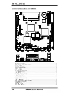
Page 11: ... the best configuration for your needs The following lists the connectors on MB860 and their respective functions Jumper Locations on MB860 8 SW1 Panel Resolution Setting 9 JP9 LCD Panel VDD Selection 9 W1 Clear CMOS Contents 9 JP2 COM1 RS232 5V 12V Power Setting 9 JP3 COM2 RS232 5V 12V Power Setting 10 JP4 COM3 RS232 5V 12V Power Setting 10 JP5 COM4 RS232 5V 12V Power Setting 10 JP6 USB Voltage S...

Page 12: ...60 Page SW1 Panel Resolution Setting 9 JP9 LCD Panel VDD Selection 9 W1 Clear CMOS Contents 9 JP2 COM1 RS232 5V 12V Power Setting 9 JP3 COM2 RS232 5V 12V Power Setting 10 JP4 COM3 RS232 5V 12V Power Setting 10 JP5 COM4 RS232 5V 12V Power Setting 10 JP6 USB Voltage Selection 10 ...

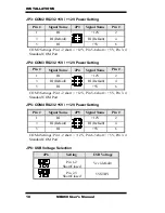
Page 13: ...efault 5V W1 Clear CMOS Contents Use this jumper to clear the CMOS contents Note that the ATX power connector should be disconnected from the board before clearing CMOS W1 Setting Function Pin 1 2 Short Closed Normal Pin 2 3 Short Closed Clear CMOS JP2 COM1 RS232 5V 12V Power Setting Pin Signal Name JP2 Signal Name Pin 1 RI 12V 2 3 RI Default RI Default 4 5 RI 5V 6 COM1 Settings Pin 1 2 short 12V ...

Page 14: ...ng Pin Signal Name JP4 Signal Name Pin 1 RI 12V 2 3 RI Default RI Default 4 5 RI 5V 6 COM3 Settings Pin 1 2 short 12V Pin 5 6 short 5V Pin 3 4 Standard COM Port JP5 COM4 RS232 5V 12V Power Setting Pin Signal Name JP5 Signal Name Pin 1 RI 12V 2 3 RI Default RI Default 4 5 RI 5V 6 COM4 Settings Pin 1 2 short 12V Pin 6 5 short 5V Pin 3 4 Standard COM Port JP6 USB Voltage Selection JP6 Setting USB Vol...

Page 15: ...onnector 14 J11 VGA CRT DB 15 connector 14 J14 RJ45 Connector 14 JV1 TV out Connector 15 CN8 Line Out Line In Mic Connector 15 FDD1 Floppy Drive Connector 15 J1 IrDA Connector 15 CN2 Digital 4 in 4 out I O Connector 16 J2 Wake On LAN Connector 16 J3 System Function Connector 16 J4 ATX Power Supply Connector 16 J5 External PS 2 Keyboard Connector 17 J8 TMDS Panel Connector 17 JP8 TV Out Connector 1...

Page 16: ...r 15 CN8 Line Out Line In Mic Connector 15 FDD1 Floppy Drive Connector 15 J1 IrDA Connector 15 CN2 Digital 4 in 4 out I O Connector 16 J2 Wake On LAN Connector 16 J3 System Function Connector 16 J4 ATX Power Supply Connector 16 J5 External PS 2 Keyboard Connector 17 J8 TMDS Panel Connector 17 JP8 TV Out Connector 17 J9 DDR SODIMM Socket 17 J10 J12 LVDS Connectors 1st channel 2nd channel 18 J13 Pan...

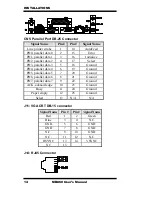
Page 17: ...ock 5 5 Mouse clock N C 6 6 N C USB1 USB Connector USB1 consists of a two stacked USB ports Refer to the section below for the respective pin assignments Pin Signal Name 1 Vcc 2 USB 3 USB 4 Ground CN4 COM1 DB 9 Serial Port Signal Name Pin Pin Signal Name DCD Data carrier detect 1 6 DSR Data set ready RXD Receive data 2 7 RTS Request to send TXD Transmit data 3 8 CTS Clear to send DTR Data terminal...

Page 18: ...ect PD3 parallel data 3 5 18 Ground PD4 parallel data 4 6 19 Ground PD5 parallel data 5 7 20 Ground PD6 parallel data 6 8 21 Ground PD7 parallel data 7 9 22 Ground ACK acknowledge 10 23 Ground Busy 11 24 Ground Paper empty 12 25 Ground Select 13 N A N A J11 VGA CRT DB 15 connector Signal Name Pin Pin Signal Name Red 1 2 Green Blue 3 4 N C GND 5 6 GND GND 7 8 GND N C 9 10 GND N C 11 12 N C HSYNC 13...

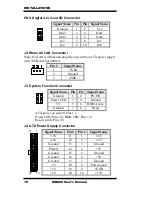
Page 19: ...ill support up to 2 88MB FDD Signal Name Pin Pin Signal Name VCC 1 2 INDEX VCC 3 4 DRV_SEL VCC 5 6 DSK_CH NC 7 8 NC NC 9 10 MOTOR DINST 11 12 DIR NC 13 14 STEP GND 15 16 WDATA GND 17 18 WGATE GND 19 20 TRACK NC 21 22 WPROT GND 23 24 RDATA GND 25 26 SIDE J1 IrDA Connector J1 is used for an optional IrDA connector for wireless communication Pin Signal Name 1 5V 2 No connect 3 Ir RX 4 Ground 5 Ir TX ...

Page 20: ...Pin Signal Name 1 5VSB 2 Ground 3 PME J3 System Function Connector Signal Name Pin Pin Signal Name Ground 1 2 PS_ON Power LED 3 4 Ground 5V 5 6 HDD Active Ground 7 8 Reset ATX power on switch Pins 1 2 Power LED Pins 3 4 HDD LED Pins 5 6 Reset switch Pins 7 8 J4 ATX Power Supply Connector Signal Name Pin Pin Signal Name 3 3V 11 1 3 3V 12V 12 2 3 3V Ground 13 3 Ground PS ON 14 4 5V Ground 15 5 Groun...

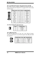
Page 21: ... Ground Default 2 3 short 4 5 short for internal CN1 keyboard For external keyboard use 1 3 5 6 pin J8 TMDS Panel Connector TMDS stands Transition Minimized Differential Signaling Signal Name Pin Pin Signal Name TX1P 1 11 TX2P TXIN 2 12 TX2N GND 3 13 GND GND 4 14 GND TXCP 5 15 TX0P TXCN 6 16 TX0N GND 7 17 NC 5v 8 18 NC HTPG 9 19 DDCDATA J8 NC 10 20 DDCCLK JP8 TV Out Connector Pin Signal Name 1 Y G...

Page 22: ...1 TX0 Ground 4 3 Ground TX1 6 5 TX1 5V 3 3V 8 7 Ground TX3 10 9 TX3 TX2 12 11 TX2 Ground 14 13 Ground TXC 16 15 TXC 5V 3 3V 18 17 ENABKL 12V 20 19 12V J13 Panel Inverter Power Connector Pin Signal Name 1 ELON 2 Ground 3 12V J15 USB Connectors The following table shows the pin outs of the USB pin headers connectors Overall the one pin header support four USB ports USB 2 0 compliant Signal Name Pin ...

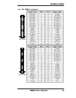
Page 23: ...t Address 1 33 34 No connect Address 0 35 36 Address 2 Chip select 0 37 38 Chip select 1 J16 IDE1 Activity 39 40 Ground Signal Name Pin Pin Signal Name Reset IDE 1 2 Ground Host data 7 3 4 Host data 8 Host data 6 5 6 Host data 9 Host data 5 7 8 Host data 10 Host data 4 9 10 Host data 11 Host data 3 11 12 Host data 12 Host data 2 13 14 Host data 13 Host data 1 15 16 Host data 14 Host data 0 17 18 H...

Page 24: ...1 CD Audio R 2 Ground 3 Ground 4 CD Audio L CN3 Serial Ports Pin Signal Name RS 232 1 DCD Data carrier detect 2 RXD Receive data 3 TXD Transmit data 4 DTR Data terminal ready 5 Ground 6 DSR Data set ready 7 RTS Request to send 8 CTS Clear to send 9 RI Ring indicator 10 No Connect ...

Page 25: ...s code and information is provided as is without warranty of any kind either expressed or implied including but not limited to the implied warranties of merchantability and or fitness for a particular purpose Name Enable_And_Set_Watchdog IN AL 1sec 255sec OUT None Enable_And_Set_Watchdog ProcNear pushax save time interval call Unlock_Chip mov cl 2Bh call Read_Reg and al NOT 10h call Write_Reg set ...

Page 26: ...INSTALLATIONS 22 MB860 User s Manual ...

Page 27: ... al al mov cl 0F6h call Write_Reg clear watchdog timer xor al al mov cl 30h call Write_Reg watchdog disabled call Lock_Chip ret Disable_Watchdog Endp Name Unlock_Chip IN None OUT None Unlock_Chip ProcNear Mov dx 4Eh mov al 87h out dx al out dx al ret Unlock_Chip Endp Name Lock_Chip IN None OUT None Unlock_Chip ProcNear mov dx 4Eh mov al 0AAh out dx al ret Unlock_Chip Endp ...

Page 28: ...ndex AL Value to write OUT None Write_Reg ProcNear pushax mov dx 4Eh mov al cl out dx al pop ax inc dx out dx al ret Write_Reg Endp Name Read_Reg IN CL register index OUT AL Value to read Read_Reg ProcNear Mov al cl mov dx 4Eh out dx al inc dx in al dx ret Read_Reg Endp ...

Page 29: ...ARRANTIES OF MERCHANTABILITY AND OR FITNESS FOR A PARTICULAR PURPOSE ifndef __W627HF_H define __W627HF_H 1 define W627_IOBASE 0x4E define W627HF_INDEX_PORT W627_IOBASE 0 define W627HF_DATA_PORT W627_IOBASE 1 define W627HF_REG_LD 0x07 define W627HF_UNLOCK 0x87 define W627HF_LOCK 0xAA void Set_W627HF_LD unsigned char void Set_W627HF_Reg unsigned char unsigned char unsigned char Get_W627HF_Reg unsign...

Page 30: ...W627HF_INDEX_PORT W627HF_UNLOCK outportb W627HF_INDEX_PORT W627HF_UNLOCK void Lock_W627HF void outportb W627HF_INDEX_PORT W627HF_LOCK void Set_W627HF_LD unsigned char LD Unlock_W627HF outportb W627HF_INDEX_PORT W627HF_REG_LD outportb W627HF_DATA_PORT LD Lock_W627HF void Set_W627HF_Reg unsigned char REG unsigned char DATA Unlock_W627HF outportb W627HF_INDEX_PORT REG outportb W627HF_DATA_PORT DATA L...

Page 31: ...W627HF H void ClrKbBuf void int main int argc char argv int main int argc char argv unsigned char ucDO 0 data for digital output unsigned char ucDI data for digital input unsigned char ucBuf Set_W627HF_LD 0x07 switch to logic device 7 Set_W627HF_Reg 0xF1 0x00 clear ucDI Get_W627HF_Reg 0xF1 0x0F ClrKbBuf while 1 ucDO Set_W627HF_Reg 0xF1 ucDO 0x0F 4 ucBuf Get_W627HF_Reg 0xF1 0x0F if ucBuf ucDI ucDI ...

Page 32: ...pter are as follows BIOS Introduction 29 BIOS Setup 29 Standard CMOS Setup 31 Advanced BIOS Features 34 Advanced Chipset Features 37 Integrated Peripherals 39 Power Management Setup 42 PNP PCI Configurations 45 PC Health Status 46 Frequency Voltage Control 47 Load Fail Safe Defaults 48 Load Setup Defaults 48 Set Supervisor User Password 48 Save Exit Setup 48 Exit Without Saving 48 ...

Page 33: ... is immediately activated Pressing the Del key immediately allows you to enter the Setup utility If you are a little bit late pressing the Del key POST Power On Self Test will continue with its test routines thus preventing you from invoking the Setup If you still wish to enter Setup restart the system by pressing the Reset button or simultaneously pressing the Ctrl Alt and Delete keys You can als...

Page 34: ...ain Menu displays the control keys for this menu At the bottom of the Main Menu just below the control keys section there is another section which displays information on the currently highlighted item in the list Note If the system cannot boot after making and saving system changes with Setup the Award BIOS supports an override to the CMOS settings that resets your system to its default Warning I...

Page 35: ... 00 Menu Level IDE Primary Master None Change the day month IDE Primary Slave None Year and century IDE Secondary Master None IDE Secondary Slave None Drive A None Drive B None Video EGA VGA Halt On All Errors Base Memory 640K Extended Memory 129024K Total Memory 130048K At the bottom of the menu are the control keys for use on this menu If you need any help in each item field you can press the F1...

Page 36: ...s Enter to configure the hard disk The selections include Auto Manual and None Select Manual to define the drive information manually You will be asked to enter the following items CYLS Number of cylinders HEAD Number of read write heads PRECOMP Write precompensation LANDZ Landing zone SECTOR Number of sectors The Access Mode selections are as follows Auto Normal HD 528MB Large for MS DOS only LBA...

Page 37: ...or not the system will halt if an error is detected during power up No errors The system boot will not be halted for any error that may be detected All errors Whenever the BIOS detects a non fatal error the system will stop and you will be prompted All But Keyboard The system boot will not be halted for a keyboard error it will stop for all other errors All But Diskette The system boot will not be...

Page 38: ...00 DBFFF Shadow Disabled DC000 DFFFF Shadow Disabled Small Logo EPA Show Enabled Allows you choose the VIRUS warning feature for IDE Hard Disk boot sector protection If this function is enabled and someone attempt to write data into this area BIOS will show a warning message on screen and alarm beep Virus Warning This item protects the boot sector and partition table of your hard disk against acci...

Page 39: ...BIOS checks for a floppy drive while booting up If it cannot detect one either due to improper configuration or its absence it will flash an error message Boot Up NumLock Status This allows you to activate the NumLock function after you power up the system Gate A20 Option This field allows you to select how Gate A20 is worked Gate A20 is a device used to address memory above 1 MB Typematic Rate Se...

Page 40: ...indows 95 98 without a floppy disk drive select Enabled to release IRQ6 This is required to pass Windows 95 98 s SCT test You should also disable the Onboard FDC Controller in the Integrated Peripherals screen when there s no floppy drive in the system If you set this feature to Disabled the BIOS will not report the missing floppy drive to Win95 98 Video BIOS Shadow This item allows you to change ...

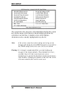
Page 41: ...CI Read Pre Fetch Enabled AC97 Read Pre Fetch Enabled PCI Slots Read Pre Fetch Enabled PCI 14M USB CLK PowerDown Disabled Phoenix AwardBIOS CMOS Setup Utility AGP Configuration AGP Aperture Size MB 128 ITEM HELP AGP 4X override Disabled Menu Level Phoenix AwardBIOS CMOS Setup Utility HyperTransport Configuration TM8000 to M1563 HTT Freq 400MHz 400MHz ITEM HELP TM8000 to M1563 HTT Width 8 Bits Menu...

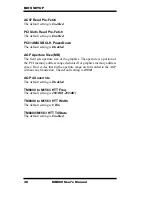
Page 42: ...the graphics The aperture is a portion of the PCI memory address range dedicated for graphics memory address space Host cycles that hit the aperture range are forwarded to the AGP without any translation The default setting is 128M AGP 4X override The default setting is Disabled TM8000 to M1563 HTT Freq The default setting is 400MHz 400MHz TM8000 to M1563 HTT Width The default setting is 8 Bits TM...

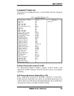
Page 43: ...ort 4 Use IRQ IRQ10 POWER ON Function BUTTON Only Hot Key Power ON Ctrl F1 Onboard FDC Controller Enabled Onboard Serial Port 1 3F8 IRQ4 Onboard Serial Port 2 2F8 IRQ3 UART Mode Select Normal RxD TxD Active Hi Lo IR Transmission Delay Enabled UR2 Duplex Mode Half Use IR Pins IR Rx2Tx2 Onboard Parallel Port 378 IRQ7 Parallel Port Mode SPP EPP Mode Select EPP1 7 ECP Mode Use DMA 3 PWRON After PWR Fa...

Page 44: ...d By default this field is set to Disabled On Chip USB2 0 Controller The options for this field are Enabled and Disabled By default this field is set to Disabled In order to use USB 2 0 necessary OS drivers must be installed first Init Display First This field allows the system to initialize first the VGA card on chip or the display on the PCI Slot By default the PCI Slot VGA is initialized first ...

Page 45: ...rts and their addresses The default values for these ports are Serial Port 1 3F8H IRQ4 Serial Port 2 2F8H IRQ3 Serial Port 3 3E8H IRQ11 Serial Port 4 2E8H IRQ10 Parallel Port 378H IRQ7 UART Mode Select This field determines the UART 2 mode in your computer The default value is Normal Other options include IrDA and ASKIR Parallel Port Mode This field allows you to determine parallel port mode funct...

Page 46: ...Mode Disabled PowerOn WakeUp Function Soft Off by PWR BTTN Instant Off WakeUp PowerOn by PCI Card Disabled WakeUp PowerOn by Ring Disabled CPU THRM Throttling 87 5 Resume by Alarm Disabled Date of Month Alarm 0 Time hh mm ss Alarm 0 0 0 Suspend Break Events IRQ 1 KeyBoard Enabled IRQ 3 Disabled IRQ 4 Disabled IRQ 5 Disabled IRQ 6 Floppy Disk Enabled IRQ 7 Disabled IRQ 8 RTC Disabled IRQ 9 Disabled...

Page 47: ...Off features There are three options V H SYNC Blank Default setting blank the screen and turn off vertical and horizontal scanning DPMS Allows BIOS to control the video display Blank Screen Writes blanks to the video buffer HDD Power Down When enabled and after the set time of system inactivity the hard disk drive will be powered down while all other devices remain active Suspend Mode When enabled...

Page 48: ...eld enables or disables the resumption of the system operation When enabled the user is allowed to set the Date and Time Suspend Break Events The HDD FDD COM LPT Ports and PCI PIRQ are I O events which can prevent the system from entering a power saving mode or can awaken the system from such a mode When an I O device wants to gain the attention of the operating system it signals this by causing a...

Page 49: ...f you need the BIOS to configure non boot devices PNP OS Installed The default setting is No Reset Configuration Data This field allows you to determine whether to reset the configuration data or not The default value is Disabled Resources Controlled by This PnP BIOS can configure all of the boot and compatible devices automatically with the use of a use a PnP operating system such as Windows 95 P...

Page 50: ...d allows the user to set the temperature so that when the temperature is reached the systems sounds a warning This function can help prevent damage to the system that is caused by overheating Temperatures Fan Speeds Voltages These fields are the parameters of the hardware monitoring function feature of the motherboard The values are read only values as monitored by the system and show the PC healt...

Page 51: ...er how to configure the processor frequency Phoenix AwardBIOS CMOS Setup Utility Frequency Voltage Control Spread Spectrum Disabled ITEM HELP Menu Level Spread Spectrum This field sets the value of the spread spectrum The default setting is Disabled This field is for CE testing use only ...

Page 52: ...ssword message prompts on the screen Type the password up to eight characters in length and press Enter The system confirms your password by asking you to type it again After setting a password the screen automatically returns to the main screen To disable a password just press the Enter key when you are prompted to enter the password A message will confirm the password to be disabled Once the pas...

Page 53: ...BIOS SETUP MB860 User s Manual 49 This page is intentionally left blank ...

Page 54: ... vendor where you made the purchase The contents of this section include the following ALi Integrated Driver Installation 51 Transmeta TM8000 AGP Driver Installation 53 Analog Device AC 97 Audio Driver Installation 55 ATI Mobility Radeon M7 M9 VGA Driver Installation 57 Realtek LAN Drivers Installation 58 IMPORTANT NOTE After installing your Windows operating system Windows 98SE ME 2000 XP you mus...

Page 55: ... the software drivers will enable Plug Play INF support for Intel chipset components Follow the instructions below to complete the installation under Windows 98SE ME 2000 XP 1 Insert the CD that comes with the motherboard and the screen below would appear Click ATI ALI Chipsets and then TM8000 ALi1563M 2 Click ALi Integrated Drivers ...

Page 56: ...DRIVER INSTALLATION 52 MB860 User s Manual 3 When the Welcome screen appears click Next to continue 4 Click Next to continue 5 The Setup process is now complete ClickOK to restart the computer ...

Page 57: ... Installation Follow the steps below to install the Transmeta TM8000 AGP driver under Windows 2000 XP 1 Insert the CD that comes with the motherboard and the screen below would appear Click ATI ALI Chipsets and then TM8000 ALi1563M 2 Click TM8X00 AGP Grant miniport Drivers ...

Page 58: ...DRIVER INSTALLATION 54 MB860 User s Manual 3 Click Next to continue 4 Click Next to continue ...

Page 59: ...DRIVERS INSTALLATION MB860 User s Manual 55 5 Click Next to continue 6 The Setup process is now complete ClickOK to restart the computer ...

Page 60: ...nstall the Analog Device AC 97 Codec Audio Driver 1 Insert the CD that comes with the motherboard and on the initial screen click ATI ALi ChipsetsèTM8000 Ali1563M Chipset DriversèAnalog Device AC 97 Codec Audio Driver 2 Click Next to continue 3 Click Continue Anyway to continue 4 Click Finish to restart the computer ...

Page 61: ...th the motherboard and the screen below would appear Click VGA Card and then ATI Mobility Radeon M7 M9 M10 series VGA Drivers 2 In the welcome screen click Next to continue the installation 3 In the license agreement window click Yes to continue 4 In the next screen click Express to start to install the drivers into the system 5 The Setup process is now complete Click Finish to restart the compute...

Page 62: ...ow the steps below to start installing the Realtek LAN drivers 1 Insert the CD that comes with the motherboard and the screen below would appear Click LAN Card and then Realtek Network Interface Controller Drivers 2 The Setup process is already complete Please restart the computer ...

Page 63: ...DRIVERS INSTALLATION MB860 User s Manual 59 This page is intentionally left blank ...

Page 64: ...05Fh Timer 060h 06Fh Keyboard Controller 070h 07Fh Real Time Clock NMI 080h 09Fh DMA Page Register 0A0h 0BFh Interrupt Controller 2 0C0h 0DFh DMA Controller 2 0F0h Clear Math Coprocessor Busy Signal 0F1h Reset Math Coprocessor 1F0h 1F7h IDE Interface 278 27F Parallel Port 2 LPT2 2F8h 2FFh Serial Port 2 COM2 2B0 2DF Graphics adapter Controller 378h 3FFh Parallel Port 1 LPT1 360 36F Network Ports 3B...

Page 65: ...ng table shows the IRQ used by the devices on board Level Function IRQ0 System Timer Output IRQ1 Keyboard IRQ2 Interrupt Cascade IRQ3 Serial Port 2 IRQ4 Serial Port 1 IRQ5 Reserved IRQ6 Floppy Disk Controller IRQ7 Parallel Port 1 IRQ8 Real Time Clock IRQ9 Reserved IRQ10 Reserved IRQ11 Reserved IRQ12 PS 2 Mouse IRQ13 80287 IRQ14 Primary IDE IRQ15 Secondary IDE ...

Reviews: