SECTION 3
CIRCUIT DESCRIPTION
3 - 1
3-1 RECEIVER CIRCUITS
3-1-1 RF AMPLIFER CIRCUIT (MAIN UNIT)
The RF circuit amplifies signals within the range of frequen-
cy coverage and filters out-of-band signals.
The signals from the antenna connector are amplified at the
RF amplifier (Q1) via the bandpass filter (L1, C3). The ampli-
fied signals are applied to the 1st mixer circuit (Q2) after out-
of-band signals are suppressed at the 3-stage of bandpass
filters (L2, L3, L4, C11, C14, C17).
3-1-2 1ST MIXER AND 1ST IF CIRCUITS
(MAIN UNIT)
The 1st mixer circuit converts the received signal into a fixed
frequency of the 1st IF signal with a PLL output frequency.
By changing the PLL frequency, only the desired frequency
will pass through a crystal filter at the next stage of the 1st
mixer.
The signals from the RF circuit are mixed at the 1st mixer
(Q2) with a 1st LO signal coming from the PLL circuit to pro-
duce a 21.7 MHz 1st IF signal.
The 1st IF signal is applied to the crystal filters (FI1, FI2) to
suppress out-of-band signals. The filtered 1st IF signal is
amplified at the 1st IF amplifier (Q3), then applied to the 2nd
mixer circuit (IC1, pin 16).
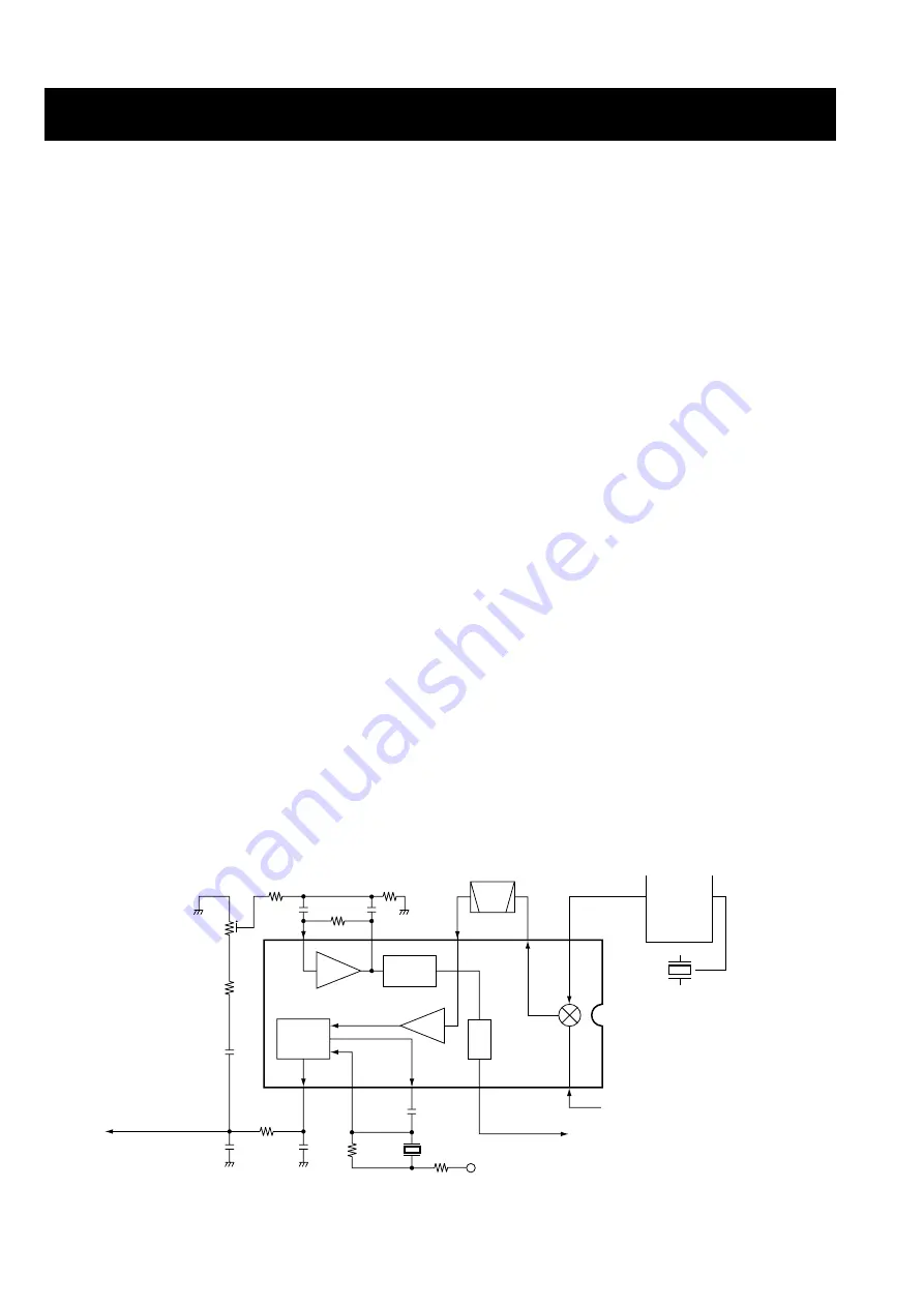
3-1-3 2ND IF AND DEMODULATOR CIRCUITS
(MAIN UNIT)
The 2nd mixer circuit converts the 1st IF signal into a 2nd IF
signal. A double conversion superheterodyne system (which
converts receive signals twice) improves the image rejection
ratio and obtains stable receiver gain.
The 1st IF signal from the IF amplifier is applied to the 2nd
mixer section of the FM IF IC (IC1, pin 16), and is mixed with
the 2nd LO signal to be converted into a 450 kHz 2nd IF sig-
nal.
The FM IF IC contains the 2nd mixer, limiter amplifier, quad-
rature detector and active filter circuits. A 2nd LO signal
(21.25 MHz) is produced at the PLL circuit using reference
frequency.
The 2nd IF signal from the 2nd mixer (IC1, pin 3) passes
through ceramic filter (FI3) to remove unwanted hetero-
dyned frequencies. It is then amplified at the limiter amplifi-
er (IC1, pin 5), and is applied to the quadrature detector
(IC1, pins 10, 11) to demodulate the 2nd IF signal into AF
signals.
3-1-4 SQUELCH CIRCUIT (MAIN UNIT)
A portion of the AF signals from the FM IF IC (IC1, pin 9) is
applied to the active filter section (IC1, pin 8) where noise
components are amplified and detected with an internal
noise detector. The squelch level adjustment pot (R29) is
connected to the active filter input (pin 8) to control the input
noise level.
The active filter section amplifies noise components. The fil-
tered signals are rectified at the noise detector section and
converted into “SQL” signal (DC voltage) at the noise com-
parator section. The “SQL” signal is output from pin 13.
This squelch circuit is only used for the BUSY detection of
Ch70, and is not related the DSC decoder sensitivity and
etc.
• 2nd IF and demodulator circuits
Mixer
16
Limiter
amp.
2nd IF filter
450 kHz
PLL IC
IC2
X2
21.25 MHz
X1
(21.25 MHz)
RSSI
IC1 TA31136FN
13
1st IF (21.7 MHz)
from Q3
"SQL" signal to the CPU
(LOGIC unit; IC1) pin 38
11
10
9
8
7
5
3
AF signal "DEMOD"
R8V
Squelch level
adjustment pot
2
17
16
Active
filter
FI3
Noise
detector
FM
detector


