4 - 3
A portion of the AF signals from the FM IF IC (IC1001, pin 9)
are applied to the active filter section (IC1001, pin 8). The
active filter section amplifies and filters noise components.
The filtered signals are applied to the noise detector section
and output from the IC1001 (pin 14) as the “L_SQL” signal.
The “L_SQL” signal from IC1001 (pin 14) is applied to the
CPU (IC2013, pin 40). The CPU analyzes the noise condition
and outputs the “L_DET_MUTE” signal to the AF mute switch
(Q1010).
• TONE SQUELCH
The tone squelch circuit detects AF signals and opens the
squelch only when receiving a signal containing a matching
subaudible tone (CTCSS). When tone squelch is in use, and
a signal with a mismatched or no subaudible tone is
received, the tone squelch circuit mutes the AF signals even
when noise squelch is open.
A portion of the AF signals from the FM IF IC (IC1001, pin 9)
passes through the low-pass filter (Q1003) to remove AF
(voice) signals. The filtered signal is applied to the CTCSS
decoder which is inside the CPU (IC2013, pin 41) via the
“L_DTCS_IN” line to control the AF mute switch (Q1010).
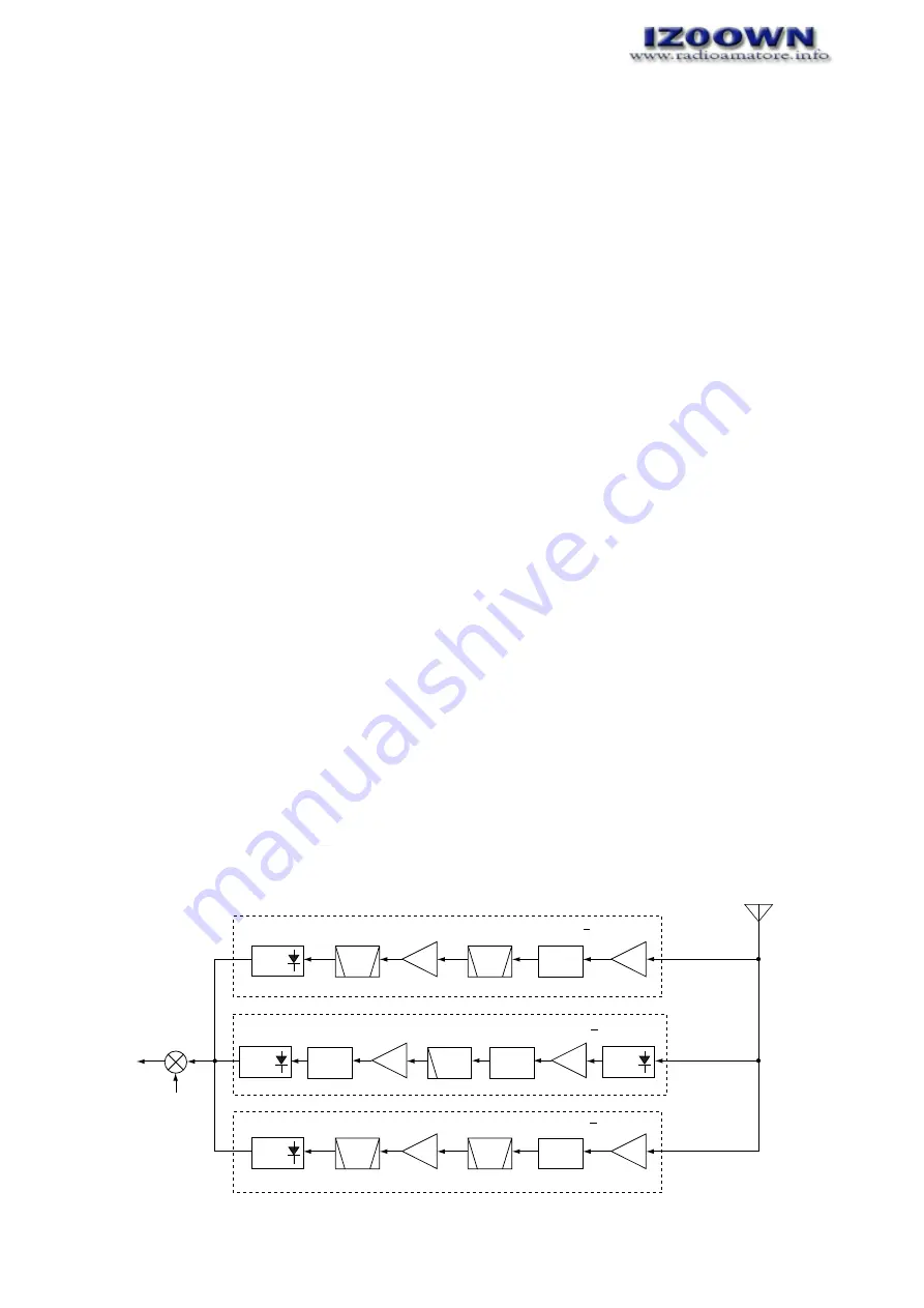
4-1-7 RF CIRCUIT FOR RIGHT SIDE DISPLAY
(MAIN UNIT)
• RF SIGNALS U-V (136 MHz–174 MHz)
The amplified signals are applied to the RF amplifier (Q30)
after being passed through the attenuator (D60) and band-
pass filter (D48, D54). The signals are applied to the RX
band switching circuit (D29) via the another bandpass filter
(D33, D40) to supress the unwanted signals.
• RF SIGNALS U-U3 (810 MHz–1000 MHz)
The signals are applied to the RF amplifier (Q18) after being
passed through the RX band switching circuit (D2061). The
amplified signals pass through the attenuator (L19, C20,
C46, C51, R178–R180) and high-pass filter (L20, C278,
C279), and are then applied to the another RF amplifier
(Q35) again. The signals pass through the attenuator (L10,
C15, C280, R183–R185) and RX bamd switching circuit
(D11).
• RF SIGNALS V-U2 (375 MHz–550 MHz)
The amplified signals are applied to the RF amplifier (Q19)
after being passed through the attenuator (D24) and band-
pass filter (D22, D72). The signals are applied to the RX
band switching circuit (D8) via the another bandpass filter
(D12, D16) to supress the unwanted signals.
The signals from the RX band swtiching circuits are then
applied to the right side displayed 1st mixer circuit (IC1006,
pin 6).
4-1-8 1ST MIXER AND 1ST IF CIRCUIT FOR RIGHT
SIDE DISPLAY (MAIN UNIT)
The 1st mixer circuit converts the received RF signals to a
fixed frequency of the 1st IF signal with a PLL output fre-
quency. By changing the PLL frequency, only the desired fre-
quency will pass through the bandpass filter at the next stage
of 1st mixer circuit.
The RF signals are mixed with 1st LO signals at the 1st mixer
(IC1006) to produce a 46.05 MHz 1st IF signal. The 1st IF
signal is output from pin 1, and passed through the crystal
bandpass filter (FI1004) to suppress unwanted harmonic
components. The filtered signal is amplified at the IF amplifi-
er (Q1041) after being passed through the limiter circuit
(D1022). The amplified signal is applied to the 2nd mixer cir-
cuit (IC1004).
4-1-9 2ND IF AND DEMODULATOR CIRCUITS FOR
RIGHT SIDE DISPLAY (MAIN UNIT)
The 2nd mixer circuit converts the 1st IF signal to a 2nd IF
signal. A double conversion superheterodyne system (which
converts receive signal twice) improves the image rejection
ratio and obtains stable receiver gain.
The FM IC IC (IC1004) contains the 2nd mixer, limiter and
noise amplifiers, quadrature detector, S-meter detector,
active filter circuits, etc. A 2nd LO signal (45.595 MHz) is pro-
duced at the PLL circuit by dividing it’s reference frequency.
BPF
BPF
ANTENNA
1st mixer
(IC1006)
1st LO
to 2nd mixer
circuit
ATT
RX
SW
RF
PRE
BPF
BPF
ATT
RX
SW
RF
PRE
HPF
ATT
ATT
RX
SW
RX
SW
D60
Q30
U-V (136 MHz 174 MHz)
U-U3 (810 MHz 1000 MHz)
V-U2 (375 MHz 550 MHz)
D29
D33, D40
D48, D54
D2061
RF
Q35
RF
Q18
D11
Q33
D24
Q19
D8
D12, D16
D22, D72
Q24
• RF CIRCUIT FOR RIGHT SIDE DISPLAY


