4 - 7
• UHF-VCO
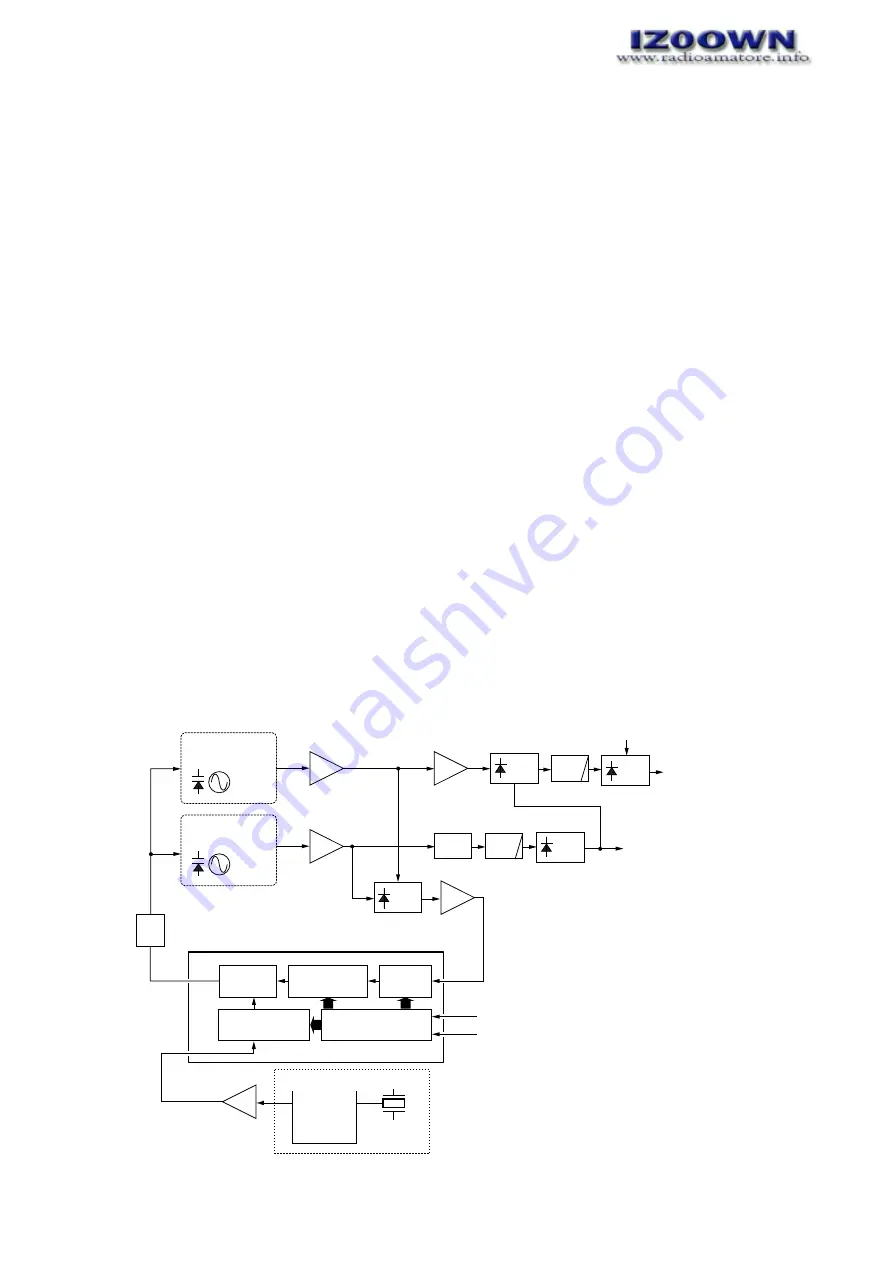
The oscillated signal at the UHF-VCO circuit is amplified at
the buffer amplifiers (Q1044, Q1047), and is then applied to
the VCO switch (D2059, D2060) to divide UHF TX signal
and RX signal.
(1) UHF TX SIGNAL
The TX UHF signal passes through the high-pass filter
(L1079, C2183, C2184) to suppress harmonics compo-
nents, and is then applied to the TX switch (D78). The sig-
nal is applied to the drive/power amplifier circuit.
(2) RX SIGNAL
The 400 MHz band RX signal is applied to the another VCO
switches (D1038 and D1049), and then passes through the
attenuator (R2206–R2208, C2122) and low-pass fiilter
(L1034, L1035, C1258). The filtered signal passes through
the VCO switch (Q1048, D1039), and is then applied to the
1st mixer circuit (IC1006, pin 4) as the 1st LO signal.
The 900 MHz band RX signal passes through the another
VCO switches (D1027 and D1028), and is then amplified at
the buffer amplifier (Q1042). The signal passes through the
attenuator (L1020, C1202, C1206) and low-pass fiilter
(L1021, L1036, C1252, C1259, C1260). The filtered signal
passes through the VCO switch (D1026), and is then
applied to the 1st mixer circuit (IC1006, pin 4) as the 1st LO
signal.
A portion of the signal from the buffer amplifier (Q1044)
passes through the VCO swtich (D1024), and is then ampli-
fied at the buffer amplifier (Q1016). The amplified signal is
fed back to the PLL IC (IC1008, pin 8) as the comparison
signal.
4-3-4 PLL CIRCUIT FOR LEFT SIDE DISPLAY
(VCO UNIT)
An oscillated signal from the L-VCO circuit passes through
the buffer amplifiers (Q7, Q1) is applied to the PLL IC for left
side display (IC1, pin 8).
And is then prescaled in the PLL IC based on the divided
ratio (N-data). The reference signal is generated at the
refenrece oscillator (X1, 12.8 MHz). The reference signal is
also applied to the PLL IC. The PLL IC detects the out-of-
step phase using the reference frequency and outputs it
from pin 16. The output signal is passed through the loop fil-
ter (Q2, Q3, D2) and is then applied to the left side display
VCO circuit as lock voltage.
4-3-5 L-VCO CIRCUIT FOR LEFT SIDE DISPLAY
(VCO AND MAIN UNITS)
• VHF TX SIGNAL
The oscillated signal at the VCO circuit is amplified at the
buffer amplifiers (Q7 and Q8), and then passes through the
low-pass filter (MAIN unit; L90, L91, C245–C247) and atten-
uator (R2216–R2218, C2134) via the VCO switch (D12,
D13). The signal is applied to the drive/power amlifier circuit
(MAIN unit) after being passed through the TX swtich (MAIN
unit; D77).
• RX SIGNAL
The oscillated signal at the VCO circuit is amplified at the
buffer amplifiers (Q7, Q8), and is then applied to the VCO
switch (D7–D9, D15). The signal is applied to the normal
oscillating signal, twice oscillating signal or harf oscillating
signal circuit.
Shift register
Prescaler
Phase
detector
Loop
filter
Programmable
divider
Programmable
reference divider
Q1038,
D1014,
D1015
VHF VCO for
right side display
Buff.
Q1016
Q1043
Buff.
Q1012
D1028
Q1020,
Q1022,
D1008
9
10
PLLCK
IC1008 (PLL IC for right side display)
PLLDATA
1
15
8
Q1038,
D1014,
D1015
VHF VCO for
right side display
LPF
ATT
Buff.
Buff.
Q1044
Buff.
Q1047
LPF
VCO
SW
D1023, D1024
VCO
SW
1st LO signal to the 1st mixer ciruict
for right side display (IC1006, pin 4)
D2059,
D2060
VCO
SW
D77, D78
to TX amplifier
circuit
from the PLL circuit
for left side display
TX
SW
PLL IC
IC1
X1
12.8 MHz
2
VCO UNIT
1
• PLL CIRCUIT FOR RIGHT SIDE DISPLAY


