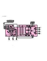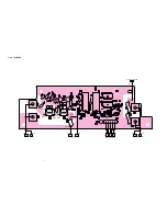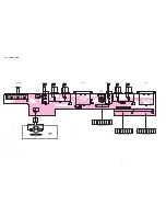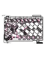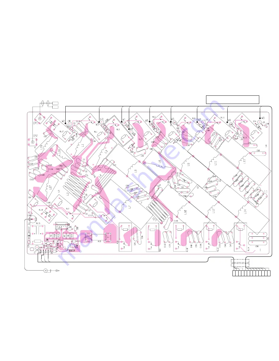
8 - 11
W12
MP6
EP7
EP6
1
13
P1
J1
TO MAIN UNIT J8
TO COMBINR UNIT
TO
SPLITER
UNIT J8
FIN
50M
24M
18M
10M
10M
14M
14M
7M
7M
35M
35M
19M
19M
GND
50M
24M
18M
GND
GND
TRU
J2
T13
EP1
EP2
FOR
REF
GND
T13
FOR
REF
GND
EP3
EP4
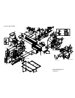
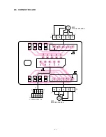
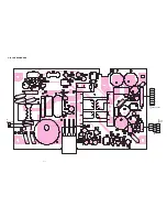
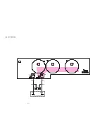
8-12 FILTER UNIT
¡
¡
TOP VIEW
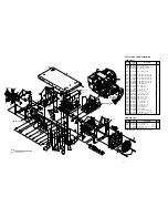
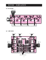
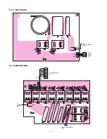
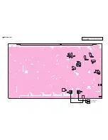
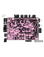
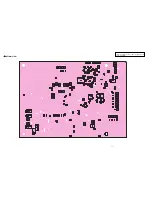
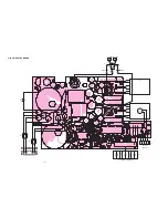
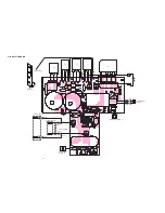
The combination of this page and the next page shows
the unit layout in the same configuration as the actual
P.C. Board.
Summary of Contents for IC-PW1
Page 1: ...SERVICE MANUAL ADDENDUM CONTENTS PARTS LIST 1 BOARD LAYOUTS 16 VOLTAGE DIAGRAM 18 Mar 2011 ...
Page 24: ...SERVICE MANUAL ADDENDUM CONTENTS PARTS LIST 1 BOARD LAYOUTS 16 Jun 2010 ...
Page 42: ...SERVICE MANUAL ADDENDUM CONTENTS PARTS LIST 1 BOARD LAYOUTS 16 VOLTAGE DIAGRAM 18 Apr 2010 ...
Page 96: ...HF 50 MHz ALL BAND LINEAR AMPLIFIER iC PW1 ...
Page 175: ...MNF F1 EP2 TO REGRELAY BOARD MLF EP1 F2 TO REGRELAY BOARD EP35 I N FG 8 19 FIL AC BOARD 8 20 ...
Page 201: ...A 5449MZ S 3 1999 Icom Inc 1 1 32 Kamiminami Hirano ku Osaka 547 0003 Japan Count on us ...

