3.8 Section 5: A/D & D/A Register
z
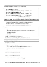
I/O address of DA-0 = wAddrAdda
z
I/O address of DA-1 = wAd 1*4
z
I/O address of FIFO = wAddrAdda
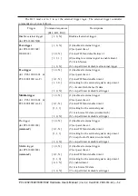
Writing data to this section will write data to the DACs and reading data from this
port will read the data from A/D FIFO. The read/write operation is given as follows:
Port Read
Write
S 0
A/D FIFO.
DAC1 write.
S 4
Reserved
DAC2 write.
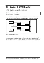
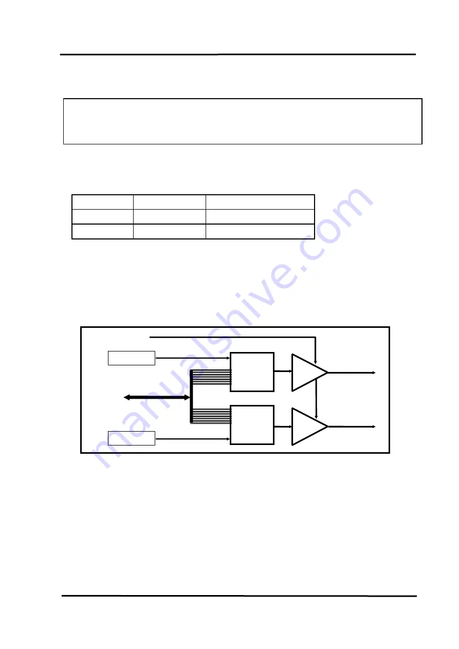
The PCI-1800/1802 provides 2 independent 12-bits D/A converters with double buffer,
bipolar voltage output. The output voltage can be
±
5 V or
±
10 V selected by J1. When the
PCI-1800/1802 is first power-on, the D/A will be in the floating state. The D/A will go to the
programmed state after executing D/A output command. The block diagram is given as below:
Figure 4-2 : D/A output diagram.
Note: The D/A output is
floating after first power-on
. The D/A output will be enabled after
executing D/A output command. This is the common feature of PCI-1202/1602/1800/1802.
Se 0
DA1
DA2
Local Data Bus
D0,D1…D11
Se 4
Vref
5 or 10
Select
Double Buffer
Analog Output 1
Analog Output2
Select
PCI-1202/1602/1800/1802 Hardware User’s Manual
(
Ver.4.2, Dec/2009, PMH-014-42)---- 64


