7. Calibration
7.1 AD Calibration
z
For PCI-1202/1800/1802
Step 1: Apply 0 V to channel 0
Step 2: Apply 4.996 V to channel 1
Step 3: Apply +0.6245 V to channel 2 for PCI-1202
(L/LU)
/1800
(L)
/1802
(L)
Step 4: Apply +4.996 mV to channel 2 for PCI-1202
(H/HU)
/1800
(H)
/1802
(H)
Step 5: Run DEMO19.EXE
Step 6: Adjust VR101 until CAL_0 = 7FF or 800
Step 7: Adjust VR100 until CAL_1 = FFE or FFF
Step 8: Repeat Step6 & Step7 until all OK
Step 9: Adjust VR1 until CAL_2 = FFE or FFF
Step 10: Adjust VR2 until CAL_3 = 000 or 001
CE
COM
Power Supply
5.0001 V
0.0001 V
0.6250 V
POWER
On
OFF
ICP DAS
Output Vlotage
OUT
CON3
CON2
PCI-1602/1602F REV:1.0
IN
CON1
VR1
VR3
VR2
VR4
J1
10V
5V
JP1
2
6
VR5 VR6 VR7
1
5
CH 0
CH 1
CH 2
CH 16
A. GND
DN-37 I/O CONNECTOR BLOCK
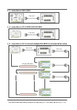
Figure 7-1. AD Calibration
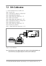
Note: The CH 16 is the GND of analog signal for PCI-1202/1602.1802 card
The CH 9/10 are the GND of analog signal for PCI-1800 card
PCI-1202/1602/1800/1802 Hardware User’s Manual
(
Ver.4.2, Dec/2009, PMH-014-42)---- 92


