1. Functional Overview > Device Architecture
8
PEB383 User Manual
July 25, 2011
Integrated Device Technology, Inc.
Confidential - NDA Required
1.3
Device Architecture
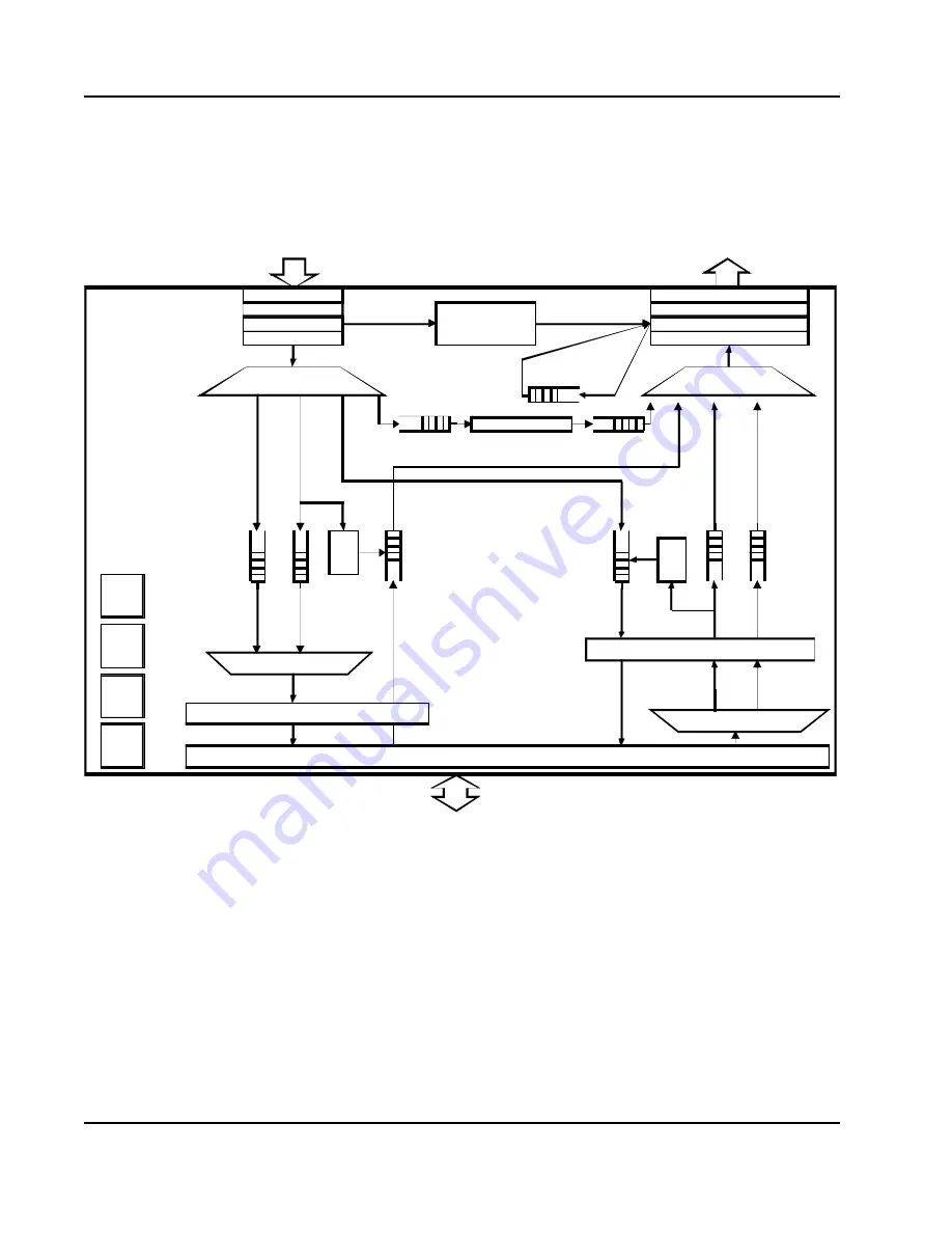
A high-level, architectural diagram of the PEB383 is displayed in
. For more information about
data flow through the device, see
Figure 2: PEB383 Device Architecture
Packets received on the PCIe Interface are processed by the data link layer and transaction layer, if
applicable. If a packet is destined for the transaction layer, its address is decoded and forwarded to the
appropriate destination:
•
Configuration register
•
Downstream posted write buffer
•
Downstream read request queue
•
Downstream read completion buffer
Rx PHY
SERDES
Con figur atio n Reg ister s
Data Link Layer
1K Replay buffers
PC Ie (Pri mary In terface)
PCI Interface (Seco nda ry Interfa ce)
Target int erface
5
1
2
(
4
e
n
tr
y
)
u
p
s
tr
e
a
m
p
o
s
te
d
w
ri
te
b
u
ffe
rs
Mast er interf ac e
Transact ion Layer
Tx PHY
SERDES
Data Link Layer
Trans ac tion Lay er
ordering
Orderi ng
Addres s decoding
PCI
Arbit er
JTAG
E EPROM
CLK/
Reset
8
e
n
tr
y
U
p
s
tr
e
a
m
R
e
a
d
R
e
q
u
e
s
t
q
u
e
u
e
Read
st ate
cac he
5
1
2
b
y
te
(
8
e
n
tr
y
)
d
o
w
n
s
tr
e
a
m
p
o
s
te
d
w
ri
te
b
u
ffe
rs
5
1
2
b
y
te
(
4
e
n
tr
y
)
d
o
w
n
s
tr
e
a
m
r
e
a
d
c
o
m
p
le
ti
o
n
b
u
ff
e
r
4
e
n
tr
y
D
o
w
n
s
tr
e
a
m
R
e
a
d
R
e
q
u
e
s
t
q
u
e
u
e
Read
st ate
c ac he
Address dec oding
Flow control
ACK/noACK
Conf ig writes & read Reques t
Conf ig reads
1
K
(
8
e
n
tr
y
)
u
p
s
tr
e
a
m
r
e
a
d
c
o
m
p
le
ti
o
n
b
u
ff
e
r


