207
PEB383 User Manual
July 25, 2011
Integrated Device Technology, Inc.
Confidential - NDA Required
14.9
PCIe and SerDes Control and Status Registers
The following table outlines the PCIe SerDes and PCS layer registers. These registers are mainly for
status reporting and testing. Caution should be taken when modifying any of these registers during
normal operation. Any unused offset space should be treated as reserved.
14.9.1
Base Offset Address Calculation
The PCIE SerDes control register addressees are calculated according to the following formula.
Address = Base + Offset
Base = 0x800
The SerDes Control and Status Registers must not be accessed if the SerDes is in reset nor
when the reference clock is stopped.
Table 38: SerDes Per-lane and Clock Control and Status Register Map
Offset
Register Name
See
“PCIe Per-Lane Transmit and Receive Registers”
0x000
PCIE_TXRX_STAT_0
“PCIe Transmit and Receive Status Register”
0x004
PCIE_OUT_STAT_0
“PCIe Output Status and Transmit Override Register”
0x008
PCIE_RX_OVRD_0
“PCIe Receive and Output Override Register”
0x00C
PCIE_DBG_CTL
“PCIe Debug and Pattern Generator Control Register”
0x02C
PCIE_PM_CTL
“PCIe Pattern Matcher Control and Error Register”
0x030
PCIE_SS_EC_CTL
“PCIe SS Phase and Error Counter Control Register”
0x034
PCIE_SCTL_FI
“PCIe Scope Control and Frequency Integrator Register”
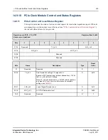
“PCIe Clock Module Control and Status Registers”
0x420
PCIE_CTL_STAT
“PCIe Control and Level Status Register”
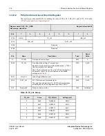
0x428
PCIE_CTL_OVRD


