IDT Test and Debug
Device Test Modes
PES12N3 User Manual
10 - 3
June 7, 2006
Notes
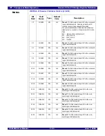
Errors on up to six lanes may be concurrently counted using the six error counters. When a lane is
selected by a Test Mode Count Lane Select (TMCNTLSEL[0..5]) and the corresponding Test Mode Count
Port Select (TMCNTPSEL[0..5]) fields in the port A Test Mode Count Configuration (TMCNTCTL) register,
then the corresponding Test Mode Error Count [0..5] (TMERRCNT[0..5]) field is incremented in the appro-
priate port A Test Mode Count (PA_TMCNT[0..3]) register whenever an error is detected.
Checking continues until the last symbol of the PRBS sequence is received. Once this occurs, checking
continues at the start of the PRBS sequence.
When a one is written to the Transmit Re-Sync (TXRS) bit in the PA_TMCTL register, the PRBS gener-
ator repeats the synchronization process described above. When a one is written to the Receive Re-Sync
(RXRS) bit in the PA_TMCTL register, the PRBS checker repeats the synchronization process described
above.
External Pseudo Random Bit Stream Self-Test Test Mode (SWMODE[3:0]
= 0xB)
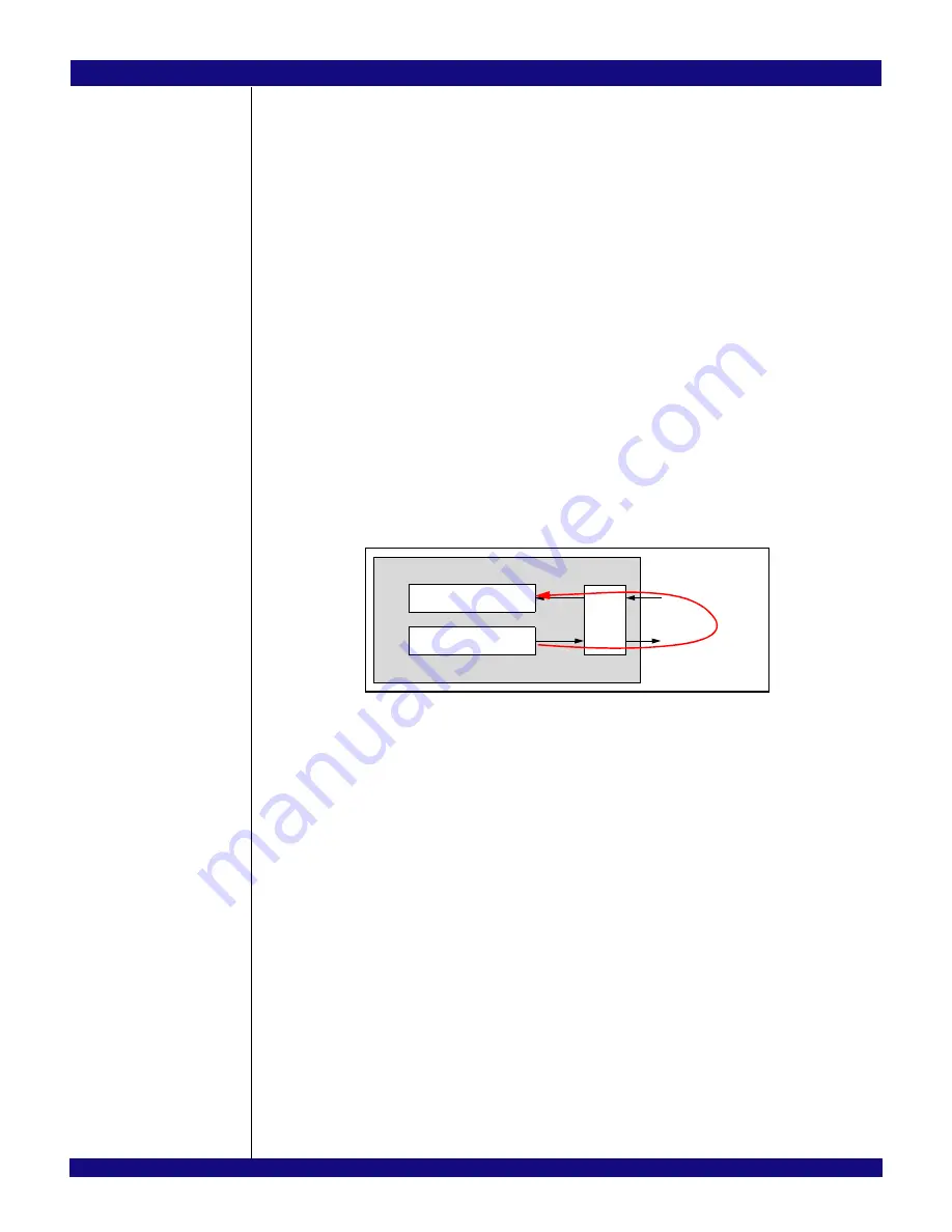
The operation of external pseudo random bit stream self-test mode is exactly the same as internal
pseudo random bit stream self-test test mode, except that the bit stream is transmitted on the SerDes lane
and is assumed to be externally looped back. This mode is graphically illustrated in Figure 10.3.
The recovered SerDes receive clock is used by the PRBS checker.
No frequency compensation is performed in this test mode. Thus, if an external bit stream generator is
used to generate the receive pattern, the same reference clock should be provided to the PES12N3 as to
the bit stream generator.
Figure 10.3 External Pseudo Random Bit Stream Self-Test
SerDes Broadcast Test Mode (SWMODE[3:0] = 0xD)
In SerDes Broadcast Test Mode, the symbols received on port C lane zero (i.e., PECRP[0] and
PECRN[0]) are broadcast, with a one 250 MHz clock cycle delay between lanes, on all lanes of the device.
This test mode uses data after 8b-10b conversion. Thus, the same reference clock should be provided to
the PES12N3 as to the bit stream generator.
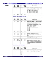
After reset, all 24-lanes of the device enter this test mode. However, individual lanes may be enabled
and disabled by setting/clearing bits in the PAEN, PBEN and PCEN fields in the port A Test Mode Control
(PA_TMCTL) register. The delay between the received pattern on port C lane zero and that transmitted on
the SerDes lanes of the device is shown in Table 10.2.
Se
rD
e
s
PES12N3
10b
PRBS Gen.
PRBS Check
Summary of Contents for 89HPES12N3
Page 10: ...IDT Table of Contents PES12N3 User Manual iv June 7 2006 Notes...
Page 14: ...IDT List of Figures PES12N3 User Manual viii June 7 2006 Notes...
Page 36: ...IDT Clocking Reset and Initialization Reset PES12N3 User Manual 2 8 June 7 2006 Notes...
Page 40: ...IDT Link Operation Slot Power Limit Support PES12N3 User Manual 3 4 June 7 2006 Notes...
Page 50: ...IDT Switch Operation Switch Core Errors PES12N3 User Manual 4 10 June 7 2006 Notes...
Page 54: ...IDT Power Management Active State Power Management PES12N3 User Manual 5 4 June 7 2006 Notes...
Page 62: ...IDT Hot Plug and Hot Swap Hot Swap PES12N3 User Manual 6 8 June 7 2006 Notes...
Page 78: ...IDT SMBus Interfaces Slave SMBus Interface PES12N3 User Manual 7 16 June 7 2006 Notes...
Page 148: ...IDT Test and Debug SerDes Test Clock PES12N3 User Manual 10 6 June 7 2006...
Page 158: ...IDT JTAG Boundary Scan Usage Considerations PES12N3 User Manual 11 10 June 7 2006 Notes...


