IDT Transparent Mode Operation
Generic PCI to PCI Bridge Register Definition
PES12N3 User Manual
9 - 47
June 7, 2006
Notes
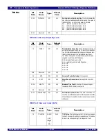
EEPROMINTF - Serial EEPROM Interface (0x0B4)
19:18
SSMBMODE
RW
0x0
Slave SMBus Mode. The slave SMBus contains internal
glitch counters on the SSMBCLK and SSMBDAT signals
that wait approximately 1uS before sampling or driving
these signals. This field allows the glitch counter time to be
reduced or entirely removed. In some systems, this may
permit high speed slave SMBus operation.
0x0 -(normal) Slave SMBus normal mode. Glitch counters
operate with 1uS delay.
0x1 -(fast) Slave SMBus interface fast mode. Glitch
counters operate with 100nS delay.
0x2 -(disabled) Slave SMBus interface with glitch counters
disabled. Glitch counters operate with zero delay which
effectively removes them.
0x3 -reserved.
21:20
MSMBMODE
RW
0x0
Master SMBus Mode. The master SMBus contains inter-
nal glitch counters on the MSMBCLK and MSMBDAT sig-
nals that wait approximately 1uS before sampling or driving
these signals. This field allows the glitch counter time to be
reduced or entirely removed. In some systems, this may
permit high speed master SMBus operation.
0x0 -(normal) Master SMBus normal mode. Glitch counters
operate with 1uS delay.
0x1 -(fast) Master SMBus interface fast mode. Glitch
counters operate with 100nS delay.
0x2 -(disabled) Master SMBus interface with glitch
counters disabled. Glitch counters operate with zero delay
which effectively removes them.
0x3 -reserved.
31:22
Reserved
RO
0x0
Reserved field.
1.
The MSMBCLK low minimum pulse width is equal to half the period programmed in this field. The value of 0x53, which corre-
sponds to~373 KHz, allows the min low pulse width to be satisfied. In systems where this timing parameter is not critical, the op-
erating frequency may be increased.
Bit
Field
Field
Name
Type
Default
Value
Description
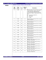
15:0
ADDR
RW
0x0
EEPROM Address. This field contains the byte address in
the Serial EEPROM to be read or written.
23:16
DATA
RW
0x0
EEPROM Data. A write to this field will initiates a serial
EEPROM read or write operation, as selected by the OP
field, to the address specified in the ADDR field.
When a write operation is selected, the value written to this
field is the value written to the serial EEPROM. When a
read operation is selected, the value written to this field is
ignored and the value read from the serial EEPROM may
be read from this field when the DONE bit is set.
Bit
Field
Field
Name
Type
Default
Value
Description
Summary of Contents for 89HPES12N3
Page 10: ...IDT Table of Contents PES12N3 User Manual iv June 7 2006 Notes...
Page 14: ...IDT List of Figures PES12N3 User Manual viii June 7 2006 Notes...
Page 36: ...IDT Clocking Reset and Initialization Reset PES12N3 User Manual 2 8 June 7 2006 Notes...
Page 40: ...IDT Link Operation Slot Power Limit Support PES12N3 User Manual 3 4 June 7 2006 Notes...
Page 50: ...IDT Switch Operation Switch Core Errors PES12N3 User Manual 4 10 June 7 2006 Notes...
Page 54: ...IDT Power Management Active State Power Management PES12N3 User Manual 5 4 June 7 2006 Notes...
Page 62: ...IDT Hot Plug and Hot Swap Hot Swap PES12N3 User Manual 6 8 June 7 2006 Notes...
Page 78: ...IDT SMBus Interfaces Slave SMBus Interface PES12N3 User Manual 7 16 June 7 2006 Notes...
Page 148: ...IDT Test and Debug SerDes Test Clock PES12N3 User Manual 10 6 June 7 2006...
Page 158: ...IDT JTAG Boundary Scan Usage Considerations PES12N3 User Manual 11 10 June 7 2006 Notes...


