background image

IDT   Transparent Mode Operation

Generic PCI to PCI Bridge Register Definition

PES12N3 User Manual

9 - 48

June 7, 2006

Notes

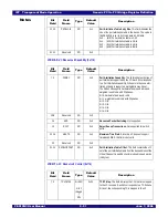
IOEXPINTF - I/O Expander Interface (0x0B8)

24

BUSY

RO

0x0

EEPROM Busy. This bit is set when a serial EEPROM 
read or write operation is in progress.
0x0 - (idle) serial EEPROM interface idle
0x1 - (busy) serial EEPROM interface operation in 

progress

25

DONE

RW1C

0x0

EEPROM Operation Completed. This bit is set when a 
serial EEPROM operation has completed.
0x0 -

(notdone) interface is idle or operation in progress

0x1 -

(done) operation completed

26

OP

RW

0x0

EEPROM Operation Select. This field selects the type of 
EEPROM operation to be performed when the DATA field 
is written
0x0 - (write) serial EEPROM write
0x1 - (read) serial EEPROM read

31:27

Reserved

RO

0x0

Reserved field.

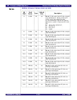
Bit  

Field

Field

Name

Type

Default

Value

Description

7:0

PBHPS

RW

0x0

Port B Hot-Plug Signals. Each bit in this field corresponds 
to a port B hot-plug signal. Reading this field returns the 
current value of the corresponding hot-plug signals (i.e., 
the input values last read from the I/O expander and output 
values supplied to the I/O expander). 
Writes to this field are ignored unless the I/O Expander 
Test Mode (IOEXTM) bit is set. When the IOEXTM bit is 
set, the value for outputs supplied to the I/O expander cor-
responds to the value written to this field instead of the 
value supplied by internal logic. Bits in this field which cor-
respond to inputs are always read-only, even when the 
IOEXTM bit is set.

15:8

PCHPS

RW

0x0

Port C Hot-Plug Signals. Each bit in this field corresponds 
to a port C hot-plug signal. Reading this field returns the 
current value of the corresponding hot-plug signals (i.e., 
the input values last read from the I/O expander and output 
values supplied to the I/O expander).
Writes to this field are ignored unless the I/O Expander 
Test Mode (IOEXTM) bit is set. When the IOEXTM bit is 
set, the value for outputs supplied to the I/O expander cor-
respond to the value written to this field instead of the value 
supplied by internal logic. Bits in this field which correspond 
to inputs are always read-only, even when the IOEXTM bit 
is set.

23:16

Reserved

RO

0x0

Reserved field.

24

RELOADIOEX

RW

0x0

Reload I/O Expander Signals. Writing a one to this field 
results in an I/O expander SMBus transaction that 
refreshes all I/O expander input and output signal values. 
This bit always returns a zero when read.

Bit  

Field

Field

Name

Type

Default

Value

Description

Summary of Contents for 89HPES12N3

Page 1: ...6024 Silver Creek Valley Road San Jose California 95138 Telephone 800 345 7015 408 284 8200 FAX 408 284 2775 Printed in U S A 2006 Integrated Device Technology Inc IDT 89HPES12N3 PCI Express Switch Us...

Page 2: ...IF IDT HAS BEEN PREVIOUSLY ADVISED ABOUT THE POSSIBILITY OF SUCH DAMAGES The code examples also may be subject to United States export control laws and may be subject to the export or import laws of...

Page 3: ...between switch ports Chapter 5 Power Management describes the power management capability structure located in the configuration space of each PCI PCI bridge in the PES12N3 Chapter 6 Hot Plug and Hot...

Page 4: ...ts either 0 or 1 the hexadecimal format is as follows 0xDD where D represents the hexadecimal digit s otherwise it is decimal The compressed notation ABC x y z D refers to ABCxD ABCyD and ABCzD The co...

Page 5: ...register bits with this attribute Reading the value will automatically cause the register bits to be reset to zero Writes cause the register bits to be modified Reserved Reserved The value read from...

Page 6: ...mation in Chapters 1 and 9 Read and Write Clear RW1C Software can read and write to registers bits with this attribute How ever writing a value of zero to a bit with this attribute has no effect A RW1...

Page 7: ...Device Overview Introduction 1 1 Features 1 3 System Identification 1 4 Vendor ID 1 4 Device ID 1 4 Revision ID 1 5 JTAG ID 1 5 Logic Diagram 1 6 Pin Description 1 7 Pin Characteristics 1 11 2 Clockin...

Page 8: ...lot 6 3 Hot Plug with Switch on an Add In Card 6 6 Hot Swap 6 7 7 SMBus Interfaces Introduction 7 1 SMBus Registers 7 2 Master SMBus Interface 7 4 Initialization 7 4 Serial EEPROM 7 4 Hot Plug I O Exp...

Page 9: ...nd Status Registers 9 40 Extended Configuration Space Access and INTx Status Registers 9 49 PCI Express Virtual Channel Capability 9 50 Test Mode Registers 9 55 System Integrity 9 60 10 Test and Debug...

Page 10: ...IDT Table of Contents PES12N3 User Manual iv June 7 2006 Notes...

Page 11: ...ration Spaces in the PES12N3 7 5 Table 7 5 PES12N3 Compatible Serial EEPROMs 7 5 Table 7 6 Serial EEPROM Initialization Errors 7 8 Table 7 7 Slave SMBus Address When a Static Address is Selected 7 9 T...

Page 12: ...IDT List of Tables PES12N3 User Manual vi June 7 2006 Notes Table 11 4 System Controller Device Identification Register 11 8...

Page 13: ...SR Register Read or Write CMD Field Format 7 11 Figure 7 7 Serial EEPROM Read or Write CMD Field Format 7 12 Figure 7 8 CSR Register Read Using SMBus Block Write Read Transactions with PEC Disabled 7...

Page 14: ...IDT List of Figures PES12N3 User Manual viii June 7 2006 Notes...

Page 15: ...essage Signaled Interrupt Address 0x080 9 39 MSICAP Message Signaled Interrupt Capability and Control 0x07C 9 39 MSIMDATA Message Signaled Interrupt Message Data 0x088 9 40 MSIUADDR Message Signaled I...

Page 16: ...ol 0x0A4 9 42 SWSICTL Switch System Integrity Control 0x500 9 60 SWSIPECNT Switch System Integrity Parity Error Count 0x504 9 61 SWSITDCNT Switch System Integrity Time Out Drop Count 0x508 9 61 SWSTS...

Page 17: ...Gbps of aggregate switching capacity through 12 integrated serial lanes using proven and robust IDT technology Each lane provides 2 5 Gbps of bandwidth in both directions The PES12N3 is fully complia...

Page 18: ...the downstream ports Port B resides on the internal PCI Bus at Device 0 Function 0 Port C resides on the internal PCI Bus at Device 1 Function 0 Type 1 Configuration Header PCI PCI Transparent Bridge...

Page 19: ...OM Highly Integrated Solution Requires no external components Incorporates on chip internal memory for packet buffering and queueing Integrates 12 2 5 Gbps embedded SerDes 8B 10B encoder decoder no se...

Page 20: ...aining and force any link into any mode Provides statistics and performance counters Two SMBus Interfaces Slave interface provides full access to all software visible registers by an external SMBus ma...

Page 21: ...during a metal mask change The revision ID shall be incremented with each all layer or metal mask change JTAG ID The JTAG ID is Version Same value as Revision ID See the Revision ID section above Part...

Page 22: ...MSMBDAT 4 SSMBADDR 5 3 1 SSMBCLK SSMBDAT 4 Master SMBus Interface Slave SMBus Interface CCLKUS RSTHALT System Pins JTAG_TDI JTAG_TDO JTAG_TMS JTAG_TRST_N JTAG Pins VSS SWMODE 3 0 4 2 2 Port A Port A...

Page 23: ...of PCI Express Port B are reversed This value may be overridden by modify ing the value of the PBLREV bit in the PA_SWCTL register PEBRP 3 0 PEBRN 3 0 I PCI Express Port B Serial Data Receive Differen...

Page 24: ...GPIO 1 I O General Purpose I O This pin can be configured as a general purpose I O pin GPIO 2 I O General Purpose I O This pin can be configured as a general purpose I O pin Alternate function pin nam...

Page 25: ...MBus should operate at 100 KHz instead of 400 kHz This value may not be overridden PERSTN I Fundamental Reset Assertion of this signal resets all logic inside the PES12N3 and initiates a PCI Express f...

Page 26: ...an logic or JTAG Controller JTAG_TRST_N I JTAG Reset This active low signal asynchronously resets the boundary scan logic and JTAG TAP Controller An external pull up on the board is recommended to mee...

Page 27: ...I LVDS Serial link PEARP 3 0 I LVDS Serial link PEATN 3 0 O LVDS Serial link PEATP 3 0 O LVDS Serial link PEBLREV I LVTTL Input pull down PEBRN 3 0 I LVDS Serial link PEBRP 3 0 I LVDS Serial link PEBT...

Page 28: ...LVTTL Input RSTHALT I LVTTL Input pull down TSTRSVD I LVTTL Input pull down External pull down SWMODE 3 0 I LVTTL Input pull up JTAG JTAG_TCK I LVTTL STI pull up JTAG_TDI I LVTTL STI pull up JTAG_TDO...

Page 29: ...figuration vector consisting of the signals listed in Table 2 2 is sampled by the PES12N3 during a fundamental reset when PERSTN is negated The boot configuration vector defines essential parameters f...

Page 30: ...ridden by modifying the SCLK bit in the PA_PCIELSTS register MSMBSMODE N Master SMBus Slow Mode The assertion of this pin indicates that the master SMBus should operate at 100 KHz instead of 400 KHz P...

Page 31: ...e to read and write regis ters internal to the device before normal device operation begins The device exits the reset state when the RSTHALT bit is cleared in the PA_SWCTL register through the SMBus...

Page 32: ...WL Y Y Y N Port B Transaction Layer Y Y Y N Port B Data Link Layer Y Y Y Y if selected Port B Phy Layer Y Y Y Y if selected Port B Downstream Hot Reset Req N Y Y Y if selected Port C All Registers Y N...

Page 33: ...uasi reset state in which the following actions occur All links enter an active Link Training state within 80ms of the clearing of the fundamental reset condition Within 100ms of the clearing of the f...

Page 34: ...side effects are initiated at the point at which the write occurs Therefore serial EEPROM initialization should be structured in a manner so as to ensure proper configuration prior to initiation of th...

Page 35: ...on page 9 25 When a globally initiated hot reset is initiated to downstream ports all of the logic associated with the transparent bridges stacks and FIFOs in the switch core associated with the down...

Page 36: ...IDT Clocking Reset and Initialization Reset PES12N3 User Manual 2 8 June 7 2006 Notes...

Page 37: ...when the REGUNLOCK bit is set in the PA_SWCTL register Modification of this field allows the maximum link width of the port to be configured The new link width takes effect the next time link training...

Page 38: ...xRP 2 PExRP 3 PES12N3 lane 0 lane 1 c x2 Port with PExLREV negated PExRP 0 PExRP 1 PExRP 2 PExRP 3 PES12N3 lane 1 lane 0 d x2 Port with PExLREV asserted PExRP 0 PExRP 1 PExRP 2 PExRP 3 PES12N3 lane 0...

Page 39: ...e to lose configuration read or write comple tions when TLPs queued in the switch are discarded 1 If this occurs the root s completion timer associated with the transaction s will time out and the tra...

Page 40: ...IDT Link Operation Slot Power Limit Support PES12N3 User Manual 3 4 June 7 2006 Notes...

Page 41: ...ons in the PES12N3 are routed through the switch core even those that could be satisfied locally due to the fact that the switch core is responsible for maintaining flow control infor mation Figure 4...

Page 42: ...ich a TLP is forwarded Associated with each TLP in an input buffer is a timestamp An egress scheduler always selects the TLP in the input buffer that contains the oldest timestamp If that TLP is desti...

Page 43: ...on defined transactions as well as those that may be used in vendor defined messages and in future revisions of the PCIe specifications Specifically the PES12N3 supports the following type of routing...

Page 44: ...ata Link DL layer of the switch ingress port the LCRC is checked and 32 bit Doubleword DWord even parity is computed on the received TLP data If an LCRC error is detected at this point the link level...

Page 45: ...ocally i e for ingress TLPs to the switch core which are consumed by the port such as Type 0 configuration read requests on the root port Switch Time Outs The switch discards any TLP that reaches the...

Page 46: ...pletion until the switch is unlocked This means that the LOCKMODE field in the PA_SWSTS register can only be read via the SMBus when the switch is locked The behavior of the switch is undefined when a...

Page 47: ...f its PCI to PCI bridge may be determined by exam ining the state of the INTA INTB INTC and INTD fields in the corresponding port s Interrupt Status PA_INTSTS PB_INTSTS and PC_INTSTS register An Asser...

Page 48: ...ion being returned to the upstream port Reception of a CfgRd0 or CfgWr0 TLP All CfgRd0 and CfgWr0 TLPs should have been received and processed by the upstream stack Therefore the upstream stack should...

Page 49: ...dge primary bus number after bus enumeration has completed There are no entities that generate accept messages on the virtual PCI bus within the switch i e the primary bus number Reception of route by...

Page 50: ...IDT Switch Operation Switch Core Errors PES12N3 User Manual 4 10 June 7 2006 Notes...

Page 51: ...ntire device When the root port enters a low power state and the PME_TO_Ack messages are received then the entire device is placed into a low power state The PES12N3 supports the following device powe...

Page 52: ...ency L1 Lower power state than L0s May be automatically entered or directed by software by placing the device in the D3hot state L2 L3 Ready The L2 L3 state is entered after the acknowledgement of a P...

Page 53: ...CI Power Management Proprietary Control PMPC register controls the amount of time L0s entry conditions must be met before the hardware transitions the link to the L0s state The L1 Entry Timer L1SET fi...

Page 54: ...IDT Power Management Active State Power Management PES12N3 User Manual 5 4 June 7 2006 Notes...

Page 55: ...upstream port serves as the add in card s PCIe interface In this application the upstream port may be hot plugged into a slot on the main system Finally Figure 6 3 illustrates the use of the PES12N3 i...

Page 56: ...Application Figure 6 3 Hot Plug with Carrier Card Application PES12N3 Port A Port B Port C Upstream Link Hot Plug Signals GPIO PCI Express Device PCI Express Device Add In Card PES12N3 Port A Port B S...

Page 57: ...hould be set during configuration in the PCI Express Slot Capabilities PCIESCAP register Table 6 7 lists the hot plug inputs and outputs that may be associated with a slot When enabled during configur...

Page 58: ...sion in IO 1 write value 0x0F to I O expander register 6 bits 4 5 6 and 7 are outputs of IO 0 write value 0x0F to I O expander register 7 bits 4 5 6 and 7 are outputs of IO 1 read value of I O expande...

Page 59: ...o the I O expander causing the value in the PBHPS and PCHPS fields to reflect the state of the I O expander signals This feature may be used to aid in debugging hot plug operation For example a user w...

Page 60: ...e then the hot plug controller generates a wake up event using a PM_PME message instead of an interrupt if the event interrupt is not masked in the slot control PCIESCTL register and hot plug interrup...

Page 61: ...xpress Device Capabilities PCIEDCAP register of the upstream port When this bit is set and GPIO 3 is configured as an alternate function the assertion of the PAABN signal results in an ATTENTION_BUTTO...

Page 62: ...IDT Hot Plug and Hot Swap Hot Swap PES12N3 User Manual 6 8 June 7 2006 Notes...

Page 63: ...pins consist of an SMBus clock pin an SMBus data pin and 4 SMBus address pins As shown in Figure 7 1 the master and slave SMBuses may be used in a unified or split configuration Figure 7 1 SMBus Inte...

Page 64: ...EPROM initialization occurs during a fundamental reset this bit is set when serial EEPROM initialization completes or when an error is detected 25 NAERR RW1C 0x0 No Acknowledge Error This bit is set i...

Page 65: ...red i e the checksum always passes 19 18 SSMBMODE RW 0x0 Slave SMBus Mode The slave SMBus contains internal glitch counters on the SSMBCLK and SSMBDAT signals that wait approximately 1uS before sampli...

Page 66: ...erial EEPROM initialization e g transparent mode with serial EEPROM initialization The address used by the SMBus interface to access the serial EEPROM is specified by the MSMBADDR 4 1 signals as shown...

Page 67: ...in double word quantities There are three configuration block types that may be stored in the serial EEPROM The first type is a single double word initialization sequence A double word initialization...

Page 68: ...ld that indicates the type of the configuration block For sequen tial double word initialization sequences this value is always 0x1 The NUMDW field specifies the number of double words initialized by...

Page 69: ...e configuration done sequence with the checksum field initialized to zero 1 The 1 s complement of this sum is placed in the checksum field The checksum is verified in the following manner An 8 bit cou...

Page 70: ...errors may occur when accessing the serial EEPROM If an error occurs then it is reported in the port A SMBus Status PA_SMBUSSTS register Software should check for errors before and after each serial...

Page 71: ...terface responds to the following SMBus transactions initiated by an SMBus master See the SMBus 2 0 specification for a detailed description of these transactions Byte and Word Write Read Block Write...

Page 72: ...nsaction indicator Setting both START and END signifies a single transaction sequence 0 Current transaction is not the last read or write sequence 1 Current transaction is the last read or write seque...

Page 73: ...f the doubleword CSR system address of register to access 4 ADDRU Address Upper Upper 6 bits of the doubleword CSR system address of register to access Bits 6 and 7 in the byte must be zero and are ig...

Page 74: ...on 0 CCODE Command Code Slave Command Code field described in Table 7 8 1 BYTCNT Byte Count The byte count field is only transmitted for block type SMBus transactions SMBus word and byte accesses do n...

Page 75: ...the NAERR bit in the PA_SMBUSSTS register The setting of this bit may indicate the following that the addressed device does not exist on the SMBus i e addressing error data is unavailable or the devic...

Page 76: ...ND S PES12N3 Slave SMBus Address Rd ADDRU A BYTCNT 5 A EEADDR CMD status A A A N DATA ADDRU A P ADDRL A S PES12N3 Slave SMBus Address Wr A N CCODE START END P PES12N3 not ready with data S PES12N3 Sla...

Page 77: ...r A CCODE START Word S PES12N3 Slave SMBus Address Rd DATALM DATALL A N P P S PES12N3 Slave SMBus Address Wr A A ADDRU A CCODE END Byte P A S PES12N3 Slave SMBus Address Wr A CCODE Byte A P A S PES12N...

Page 78: ...IDT SMBus Interfaces Slave SMBus Interface PES12N3 User Manual 7 16 June 7 2006 Notes...

Page 79: ...te function as defined in Table 8 2 When a bit is cleared to a zero the correspond ing GPIO pin operates as a general purpose I O pin 15 8 GPIOCFG RW 0x0 GPIO Configuration Each bit in this field cont...

Page 80: ...e in this field corresponds to the value of the pin irre spective of whether the pin is configured as a GPIO input GPIO output or alternate function GPIO Pin Configured as an Output When configured as...

Page 81: ...section Port Configuration Space Organization on page 9 6 The functional operation of the PES12N3 in transparent mode is fully consistent with that described in the PCI Express Base Specification revi...

Page 82: ...on of legacy interrupts or MSIs The downstream ports ports B and C do support generation of legacy interrupts and MSIs by their corresponding hot plug controllers When configured to generate INTx mess...

Page 83: ...able error processing Table 9 2 Physical Layer Errors Error Condition PCIe Base 1 0a Specification Section Action Taken TLP ending in ENDB with LCRC that does not match inverted calculated LCRC 3 5 3...

Page 84: ...nsupported request 2 3 1 2 8 Not applicable The PES12N3 never gener ates non posted transactions Unsupported request 2 3 1 See section Switch Core Errors on page 4 8 Unexpected completion 2 3 2 Non fa...

Page 85: ...uals LENGTH 4 when a packet does not contain ECRC Completion with data The packet length is correct Number of doublewords received equals LENGTH 3 when a packet does not contain ECRC Number of doublew...

Page 86: ...and may limit the utility of multiple outstanding PCIe configuration accesses For example a configuration access that modifies a secondary or subordinate bus number which is immediately followed by a...

Page 87: ...ucture 0xFFF 0x100 0x070 0x040 0x000 PCI Configuration Space 64 DWords PCI Express Extended Configuration Space 960 DWords Virtual Channel Capability Structure PCI Power Management Capability Structur...

Page 88: ...page 9 19 0x00C Byte PA_CLS CLS Cache Line Size 0x00C on page 9 20 0x00D Byte PA_PLTIMER PLTIMER Primary Latency Timer 0x00D on page 9 20 0x00E Byte PA_HDR HDR Header Type Register 0x00E on page 9 20...

Page 89: ..._PMCAP PMCAP PCI Power Management Capabilities 0x070 on page 9 36 0x074 DWord PA_PMCSR PMCSR PCI Power Management Control and Status 0x074 on page 9 36 0x078 DWord PA_PMPC PMPC PCI Power Management Pr...

Page 90: ...0x114 on page 9 51 0x118 DWord PA_VCR0STS VCR0STS VC Resource 0 Status 0x118 on page 9 52 0x120 DWord PA_VCR0TBL0 VCR0TBL0 VC Resource 0 Arbitration Table Entry 0 0x120 on page 9 53 0x124 DWord PA_VCR...

Page 91: ...0x008 Byte PB_RID RID Revision Identification 0x008 on page 9 19 0x009 3 Bytes PB_CCODE CCODE Class Code 0x009 on page 9 19 0x00C Byte PB_CLS CLS Cache Line Size 0x00C on page 9 20 0x00D Byte PB_PLTIM...

Page 92: ...04C DWord PB_PCIELCAP PCIELCAP PCI Express Link Capabilities 0x04C on page 9 30 0x050 Word PB_PCIELCTL PCIELCTL PCI Express Link Control 0x050 on page 9 30 0x052 Word PB_PCIELSTS PCIELSTS PCI Express...

Page 93: ...9 53 0x124 DWord PB_VCR0TBL1 VCR0TBL1 VC Resource 0 Arbitration Table Entry 1 0x124 on page 9 54 0x200 0x414 Reserved 0x500 Dword PB_SWSICTL SWSICTL Switch System Integrity Control 0x500 on page 9 60...

Page 94: ...n page 9 19 0x00C Byte PC_CLS CLS Cache Line Size 0x00C on page 9 20 0x00D Byte PC_PLTIMER PLTIMER Primary Latency Timer 0x00D on page 9 20 0x00E Byte PC_HDR HDR Header Type Register 0x00E on page 9 2...

Page 95: ...us 0x052 on page 9 31 0x054 DWord PC_PCIESCAP PCIESCAP PCI Express Slot Capabilities 0x054 on page 9 32 0x058 Word PC_PCIESCTL PCIESCTL PCI Express Slot Control 0x058 on page 9 33 0x05A Word PC_PCIESS...

Page 96: ...4 0x200 0x414 Reserved 0x500 Dword PC_SWSICTL SWSICTL Switch System Integrity Control 0x500 on page 9 60 0x504 Dword PC_SWSIPECNT SWSIPECNT Switch System Integrity Parity Error Count 0x504 on page 9 6...

Page 97: ...ridge does not respond to I O accesses from the primary bus specified by IOBASE and IOLIMIT 0x0 disable Disable I O space 0x1 enable Enable I O space 1 MAE RW 0x0 Memory Access Enable When this bit is...

Page 98: ...applicable 10 INTXD RW 0x0 INTx Disable Controls the ability of the PCI PCI bridge to generate an INTx interrupt message 15 11 Reserved RO 0x0 Reserved field Bit Field Field Name Type Default Value De...

Page 99: ...0x0 Detected Parity Error This bit is set by the bridge when ever it receives a poisoned TLP on the primary side regard less of the state of the PERRE bit in the PCI Command register For downstream p...

Page 100: ...software This field is implemented for compatibility with legacy soft ware Bit Field Field Name Type Default Value Description 7 0 PLTIMER RO 0x00 Primary Latency Timer Not applicable Bit Field Field...

Page 101: ...onnected Bit Field Field Name Type Default Value Description 7 0 SUBUSN RW 0x0 Subordinate Bus Number The Subordinate Bus Number register is used to record the bus number of the highest numbered PCI b...

Page 102: ...ity Error Response Enable bit in the Bridge Control register If the Parity Response Enable bit is cleared then this bit is never set Otherwise this bit is set if the secondary side of the bridge forwa...

Page 103: ...to control the forwarding of non prefetchable transactions between the primary and secondary interfaces of the bridge This field contains A 31 20 of the highest address with A 19 0 assumed to be 0xF_...

Page 104: ...contains A 31 20 of the highest memory address with A 19 0 assumed to be 0xF_FFFF that is below the primary interface of the bridge PMLIMITU speci fies the remaining bits Bit Field Field Name Type Def...

Page 105: ...e head of the capabilities structure Bit Field Field Name Type Default Value Description 31 0 EROMBASE RO 0x0 Expansion ROM Base Address The bridge does not implement an expansion ROM Thus this field...

Page 106: ...vice Con trol register for errors to be reported on the primary inter face 0x0 ignore Do not forward errors from the secondary to the primary interface 0x1 report Enable forwarding of errors from seco...

Page 107: ...function number to extend the num ber of outstanding transactions allowed by logically com bining unclaimed function numbers The value is hardwired to 0x0 to indicate that no function number bits are...

Page 108: ...mit Value and is set via a Set_Slot_Power_Limit message 0 v1 1 0x 1 v1p1 0 1x 2 v0p01 0 01x 3 v0p001x 0 001x 31 28 Reserved RO 0x0 Reserved Bit Field Field Name Type Default Value Description 0 CEREN...

Page 109: ...ct on the behavior of the transparent bridge 15 Reserved RO 0x0 Reserved field Bit Field Field Name Type Default Value Description 0 CED RW1C 0x0 Correctable Error Detected This bit indicates the stat...

Page 110: ...ss link This field depends on whether a common or separate reference clock is used When separate clocks are used 1 s to 2 s is reported with a read only value of 0x5 When a common clock is used 256 ns...

Page 111: ...ing with a distributed common reference clock 7 ESYNC RW 0x0 Extended Sync When set this bit forces transmission of 4096 FTS ordered sets in the L0s state followed by a single SKP ordered set 15 8 Res...

Page 112: ...of zero when the SLOT bit in the PCIECAP register is cleared 5 HPS RWL 0x0 Hot Plug Surprise When set this bit indicates that a device present in the slot may be removed from the system without notic...

Page 113: ...T bit in the PCIECAP register is cleared Bit Field Field Name Type Default Value Description 0 ABPE RW 0x0 Attention Button Pressed Enable This bit when set enables generation of a Hot Plug interrupt...

Page 114: ...zero when the cor responding capability is not enabled in the PCIESCAP reg ister This field is always zero if the ATTIP bit is cleared in the PCIESCAP register 0x0 reserved Reserved 0x1 on On 0x2 blin...

Page 115: ...n the Power Controller detects a power fault 2 MRLSC RW1C 0x0 MRL Sensor Changed Set when an MRL Sensor state change is detected 3 PSD RW1C 0x0 Presence Detected Changed Set when a Presence Detected c...

Page 116: ...LK RO 0x0 PME Clock Does not apply to PCI Express 20 Reserved RO 0x0 21 DEVSP RWL 0x0 Device Specific Initialization The value of zero indicates that no device specific initialization is required 24 2...

Page 117: ...ing a PME message but the port is not itself generating a PME 21 16 Reserved RO 0x0 22 B2B3 RO 0x0 B2 B3 Support Does not apply to PCI Express 23 BPCCE RO 0x0 Bus Power Clock Control Enable Does not a...

Page 118: ...generally used to read this field rather than Con figuration Reads L0 6 d0 L0s_entry 6 d1 L0s 6 d2 L1pcipm_0 6 d3 L1pcipm_1 6 d4 L1pcipm_2 6 d5 L1pcipm_3 6 d6 L1pcipm_4 6 d7 L1pcipm_5 6 d8 L1pcipm_6...

Page 119: ...5 8 NXTPTR RO 0x0 Next Pointer This field contains a pointer to the next capability structure This field is set to 0x0 indicating that it is the last capability 16 EN RW 0x0 Enable This bit enables MS...

Page 120: ...en when a MSI is signalled 31 16 Reserved RO 0x0 Reserved Bit Field Field Name Type Default Value Description 3 0 SWMODE RO HWINIT Switch Mode The value of this field encodes the switch mode sampled o...

Page 121: ...lable for general software use A hot reset does not result in modification of this field 18 17 LOCKMODE RO 0x0 Lock Mode This field reflects the current locked status of the switch 0x0 unlocked switch...

Page 122: ...as no effect This field always returns a value of zero when read 1 RSTHALT RW HWINIT Reset Halt When this bit is set all of the switch logic except the SMBus interface remains in a reset state In this...

Page 123: ...is bit take effect the next time link training occurs 6 PCLREV RW HWINIT Port C Lane Reversal When this bit is set the lanes asso ciated with port C are reversed The initial value of this reg ister co...

Page 124: ...lock divided by 40 0x12 lane18 Lane 18 recovered clock divided by 40 0x13 lane19 Lane 19 recovered clock divided by 40 0x14 0x17 Reserved 0x18 serdes0 SerDes 0 250 MHz clock output divided by four Thi...

Page 125: ...by the alternate function 23 16 GPIOD RW HWINIT GPIO Data Each bit in this field controls the corresponding GPIO pin Reading this field returns the current value of each GPIO pin regardless of GPIO pi...

Page 126: ...ROM initialization or when a configuration done command is not found in the serial EEPROM 29 URIA RW1C 0x0 Unmapped Register Initialization Attempt This bit is set if an attempt is made to initialize...

Page 127: ...r SMBus operation 0x0 normal Master SMBus normal mode Glitch counters operate with 1uS delay 0x1 fast Master SMBus interface fast mode Glitch counters operate with 100nS delay 0x2 disabled Master SMBu...

Page 128: ...es to this field are ignored unless the I O Expander Test Mode IOEXTM bit is set When the IOEXTM bit is set the value for outputs supplied to the I O expander cor responds to the value written to this...

Page 129: ...he correspond ing I O expander SMBus transaction updating the I O expander outputs completes Bit Field Field Name Type Default Value Description 0 INTA RO 0x0 INTA Aggregated State Aggregated port sta...

Page 130: ...ATA register then reads from ECFGDATA return zero and writes are ignored When the ECFGADDR register points to itself writes to the ECFGDATA register modify the con tents of the ECFGADDR register SMBus...

Page 131: ...is supported multiple bits may be set The PES12N3 supports hardware fixed round robin and weighted round robin with 32 phases bit 0 hardware fixed round robin bit 1 weighted round robin with 32 phases...

Page 132: ...ssible values of this field is a number that corre sponds to one of the asserted bits in the Port Arbitration Capability field of the VC resource 23 20 Reserved RO 0x0 26 24 VCID RO 0x0 VC ID This fie...

Page 133: ...rt arbitration period 11 10 PHASE5 RW 0x0 Phase 5 This field contains the port ID for the correspond ing port arbitration period 13 12 PHASE6 RW 0x0 Phase 6 This field contains the port ID for the cor...

Page 134: ...d contains the port ID for the corre sponding port arbitration period 13 12 PHASE22 RW 0x0 Phase 22 This field contains the port ID for the corre sponding port arbitration period 15 14 PHASE23 RW 0x0...

Page 135: ...n the test mode When the switch is in a SerDes test mode and a bit in this field is cleared then the corresponding lane does not participate in the test mode and the value received on the SerDes input...

Page 136: ...Des test mode the lane is enabled in the TMCTL register and an error is detected on a lane then the corresponding bit in this field is set 15 8 PBTF RW1C 0x0 Port B Test Failure Each bit in this field...

Page 137: ...f the Test Mode Count 0 TMCNT0 register 4 3 TMCNTPSEL0 RW 0x0 Test Mode Count Port Select 0 In SerDes test mode this field selects the port for which SerDes lane failures are counted in the the Test M...

Page 138: ...0 TMCNTLSEL4 RW 0x0 Test Mode Count Lane Select 4 In SerDes test mode this field selects which SerDes lane of the port specified in the TMCNTPSEL4 field for which failures are counted in the Test Mode...

Page 139: ...PSEL1 and TMCNTLSEL1 fields in the TMCNTCFG register then the value in this field in incremented This counter saturates at its maximum value This field is atomically cleared when read Bit Field Field...

Page 140: ...to End Parity Checking When this bit is set end to end parity is not checked by the port and errors are never generated End to end parity is always computed for data sent by the port to the switch co...

Page 141: ...ld is at its maximum value of 0xFF This counter saturates at its maximum value Reading this field causes it to be cleared 31 8 Reserved RO 0x0 Bit Field Field Name Type Default Value Description 7 0 P...

Page 142: ...IDT Transparent Mode Operation Generic PCI to PCI Bridge Register Definition PES12N3 User Manual 9 62 June 7 2006 Notes...

Page 143: ...the transmitted bit stream of any of the 24 lanes to be inverted This capability may be used to validate the correct operation of the following test modes i e validate that a test mode does in fact co...

Page 144: ...a PRBS operating at the SerDes bit clock followed by a 10 bit shift register The 10 bit symbol produced is the output of this shift register every 10 bit clocks The first 10 symbols produced in the PR...

Page 145: ...e same as internal pseudo random bit stream self test test mode except that the bit stream is transmitted on the SerDes lane and is assumed to be externally looped back This mode is graphically illust...

Page 146: ...L K J I H G F E D C B A 18 S M L K J I H G F E D C B A 19 T N M L K J I H G F E D C B A 20 U O N M L K J I H G F E D C B A 21 V P O N M L K J I H G F E D C B A 22 W Q P O N M L K J I H G F E D C B A 2...

Page 147: ...on the 2 5 GHz recovered SerDes receive clock from any of the 24 lanes divided by 40 i e 62 5 MHz may be selected SerDes Test Clock 0 TSTCLK0 is an alternate function of GPIO 6 The clock output on thi...

Page 148: ...IDT Test and Debug SerDes Test Clock PES12N3 User Manual 10 6 June 7 2006...

Page 149: ...t mode Test Access Point The system logic utilizes a 16 state six bit TAP controller a four bit instruction register and five dedi cated pins to perform a variety of functions The primary use of the J...

Page 150: ...ut JTAG RESET Asynchronous reset for JTAG TAP controller internal pull up JTAG_TCK Input JTAG Clock Test logic clock JTAG_TMS and JTAG_TDI are sampled on the rising edge JTAG_TDO is output on the fall...

Page 151: ...N 7 0 I PEBRP 7 0 I PEBTN 7 0 O PEBTP 7 0 O PECLREV I PECRN 7 0 I PECRP 7 0 I PECTN 7 0 O PECTP 7 0 O PEREFCLKN 1 0 I PEREFCLKP 1 0 I REFCLKM I VTTPE I SMBus MSMBADDR 4 1 I MSMBCLK I O MSMBDAT I O SSM...

Page 152: ...troller passes through the UPDATE IR state whatever value that is currently held in the boundary scan register s output latches is immediately transferred to the corresponding outputs or output enable...

Page 153: ...when EXTEST is disabled When the Output Enable Cell is driving a high out to the pad which enables the pad for output and EXTEST is disabled the Capture Cell will be configured to capture output data...

Page 154: ...scanning The Instruction register is comprised of 6 bits to decode instructions as shown in Table 11 3 Instruction Definition Opcode EXTEST Mandatory instruction allowing the testing of board level in...

Page 155: ...he BYPASS register is updated to be 0 If the device being used does not have a DEVICE_ID register then the BYPASS instruction will automat ically be selected into the instruction register whenever the...

Page 156: ...controller reset When the DEVICE_ID instruction is active and the TAP controller is in the Shift DR state the thirty two bit value that will be shifted out of the device ID register is 0x00022067 VAL...

Page 157: ...is best to either drive a zero on the JTAG_TCK pin when it is not being used or to use an external pull down resistor In order to guarantee that the JTAG does not interfere with normal system operatio...

Page 158: ...IDT JTAG Boundary Scan Usage Considerations PES12N3 User Manual 11 10 June 7 2006 Notes...

Reviews: