Notes
PES12N3 User Manual
4 - 1
June 7, 2006
Chapter 4
Switch Operation
Introduction
The PES12N3 utilizes an input buffered cut-through switch to forward PCIe® TLPs between switch
ports. At a high level the switch may be viewed as consisting of three PCIe stacks and a switch core. The
PCIe stacks are each responsible for performing the per port Phy, data link and transaction layer functions
defined in the PCIe specification. The switch core is responsible for maintaining routing information in route
map tables, maintaining per port ingress and egress flow control information, buffering TLPs, and
forwarding TLPs between stacks.
An architectural block diagram of the PES12N3 and switch core is provided in Figure 1.2 of Chapter 1.
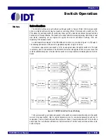
The buffering and data flow of the switch is graphically depicted in Figure 4.1 below.
Note that an ingress stack can transfer a TLP to its own egress stack through the switch core. This path
is necessary since all transactions in the PES12N3 are routed through the switch core, even those that
could be satisfied locally, due to the fact that the switch core is responsible for maintaining flow control infor-
mation.
Figure 4.1 PES12N3 Switch Data Flow and Buffering
TLPs are received by a port stack and passed to the switch core. Associated with each port in the switch
core are three input buffers. One for posted transactions, one for non-posted transactions and one for
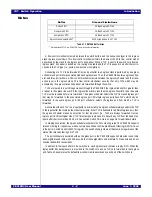
completions. The size of each of these buffers is shown in Table 4.1. Associated with each TLP in a buffer is
a descriptor. Thus, a buffer has a limitation on the total number of TLPs that can be stored as well as on the
number of bytes.
Posted FIFO
Replay Buffer
Port A Stack
Egress Functions
Port A Stack
Ingress Functions
Non-Posted FIFO
Completion FIFO
Port A
Link
Input
Port A
Link
Output
Posted FIFO
Replay Buffer
Port B Stack
Egress Functions
Port B Stack
Ingress Functions
Non-Posted FIFO
Completion FIFO
Port B
Link
Input
Port B
Link
Output
Posted FIFO
Replay Buffer
Port C Stack
Egress Functions
Port C Stack
Ingress Functions
Non-Posted FIFO
Completion FIFO
Port C
Link
Input
Port C
Link
Output
Summary of Contents for 89HPES12N3
Page 10: ...IDT Table of Contents PES12N3 User Manual iv June 7 2006 Notes...
Page 14: ...IDT List of Figures PES12N3 User Manual viii June 7 2006 Notes...
Page 36: ...IDT Clocking Reset and Initialization Reset PES12N3 User Manual 2 8 June 7 2006 Notes...
Page 40: ...IDT Link Operation Slot Power Limit Support PES12N3 User Manual 3 4 June 7 2006 Notes...
Page 50: ...IDT Switch Operation Switch Core Errors PES12N3 User Manual 4 10 June 7 2006 Notes...
Page 54: ...IDT Power Management Active State Power Management PES12N3 User Manual 5 4 June 7 2006 Notes...
Page 62: ...IDT Hot Plug and Hot Swap Hot Swap PES12N3 User Manual 6 8 June 7 2006 Notes...
Page 78: ...IDT SMBus Interfaces Slave SMBus Interface PES12N3 User Manual 7 16 June 7 2006 Notes...
Page 148: ...IDT Test and Debug SerDes Test Clock PES12N3 User Manual 10 6 June 7 2006...
Page 158: ...IDT JTAG Boundary Scan Usage Considerations PES12N3 User Manual 11 10 June 7 2006 Notes...


