5. I2C/EEPROM
133
PowerSpan II User Manual
80A1010_MA001_09
Integrated Device Technology
www.idt.com
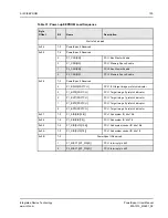
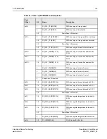
0x29
7
PB_SI0_CTL[MODE]
PB Slave image 0 image select
6
PB_SI0_CTL[DEST]
PB Slave image 0 destination
5-0
PowerSpan II Reserved
0x2A
7
PB_SI0_CTL[PRKEEP]
PB Slave image 0 image prefetch read keep
6-5
PB_SI0_CTL[END]
PB Slave image 0 image endian conversion
4-3
PowerSpan II Reserved
2-0
PB_SI0_CTL[RD_AMT]
PB Slave image 0 Read Prefetch Amount
0x2B
7-0
PB_SI0_TADDR[31:24]
PB Slave image 0 translation address bits
31-24
0x2C
7-0
PB_SI0_TADDR[23:16]
PB Slave image 0 translation address bits
23:16
0x2D
7-4
PB_SI0_TADDR[15:12]
PB Slave image 0 translation address bits
15-12
3
PB_SI0_TADDR[M3]
PB Slave image 0 master 3 select
2
PB_SI0_TADDR[M2]
PB Slave image 0 master 2 select
1
PB_SI0_TADDR[M1]
PB Slave image 0 master 1 select
0
PowerSpan II Reserved
0x2E
7-0
PB_SI0_BADDR[31:24]
PB Slave image 0 base address bits 31-24
0x2F
7-0
PB_SI0_BADDR[23:16]
PB Slave image 0 base address bits 23-16
0x30
7-4
PB_SI0_BADDR[15:12]
PB Slave image 0 base address bits 15-12
3-0
PowerSpan II Reserved
0x31
7-0
PB_REG_ADDR[31:24]
PB Slave register image base address bits
31-24
0x32
7-0
PB_REG_ADDR[23:16]
PB Slave register image base address bits
23-16
0x33
7-4
PB_REG_ADDR[15:12]
PB Slave register image base address bits
15-12
3-2
PowerSpan II Reserved
0
PB_REG_ADDR[END]
PB Slave register image endian conversion
0x34
7-0
P2_ID[DID[15:8]]
PCI-2 Device ID bits 15-8
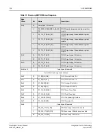
Table 31: Power-up EEPROM Load Sequence
Byte
Offset
Bit
Name
Description


