9. Resets, Clocks and Power-up Options
173
PowerSpan II User Manual
80A1010_MA001_09
Integrated Device Technology
www.idt.com
•
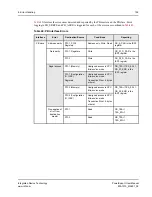
PWRUP_PRI_PCI
— PCI-1 is always the Primary Interface
9.3.1
Multiplexed System Pin Mode
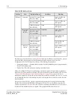
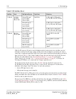
PowerSpan II multiplexes a number of pins to provide either power-up options or other system
application purposes (see
). The multiplexed system pins mode is the default mode for
PowerSpan II power-up options.
9.3.1.1
Signal Timing Requirements
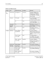
PWRUP_PB_ARB_EN, PWRUP_P1_ARB_EN, and PWRUP_P2_ARB_EN have multiple purposes:
determines the PLL frequency range, and the PowerSpan II power-up option.
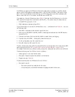
During the low to high transition of PO_RST_, the following pins are latched by PowerSpan II in order
to choose the following internal clock PLL frequency range:
•
PB_FAST Signal
— High when the PB clock frequency is between 50 MHz and 100 MHz
— Low when the PB clock frequency is between 25 MHz and 50 MHz
•
P1_M66EN Signal
— High when the PCI-1 clock frequency is 66 MHz
— Low when the PCI-1 clock frequency is 33 MHz
•
P2_M66EN signal
— High when the PCI-2 clock frequency is 66 MHz
— Low when the PCI-2 clock frequency is 33 MHz
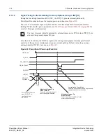
There is a 10 ns minimum input setup time and 10 ns maximum input hold time requirement for
latching these frequency range pins for determining the PLL range (see
and
, parameters
t
110
and
t
111
for more AC Timing reset information).
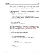
The arbiter enable and disable (PWR_PB_ARB_EN and PWRUP_P1_ARB_EN) power- up options
are sampled continuously 10 ns the negation of PO_RST_ until the power-up option is updated by the
Configuration Slave mode settings (this is only true in MPC8260 applications). The option is
determined by the logic level of PB_FAST, P1_66EN, and P2_66EN signals through internal
combination logic. This means the system can enable/disable arbiter(s) by controlling these frequency
range pins’ logic level during normal system operation after the negation of PO_RST_ if the
PB_RSTCONF signal is tied to 1 (it never goes low).

