9. Resets, Clocks and Power-up Options
174
PowerSpan II User Manual
80A1010_MA001_09
Integrated Device Technology
www.idt.com
9.3.1.2
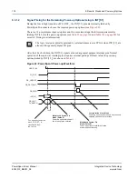
Signal Timing for the Remaining Power-up Options Using to INT[5:1]
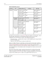
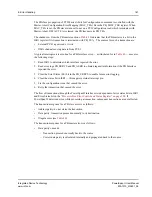
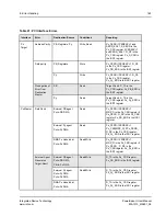
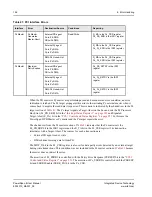
During the low to high transition of PO_RST_, the INT[5:1] pins are internally latched by
PowerSpan II in order to choose the required power-up options (see
There is a 10 ns minimum input setup time and 10 ns maximum input hold time requirement for
latching INT[5:1] for the power-up options (see
for
more AC Timing reset information).
After the 10 ns hold time, the INT[5:1] signals are used as general purpose interrupt pins. Normal
operation of these pins (as interrupt pins) requires external pull-ups. Default values for power-up
options loaded by INT[5:1]_ are shown in
Figure 22: PowerSpan II Power-up Waveform
Ti
p
The logic levels are typically provided by external transceiver or FPGA. when INT[5:1] are
also used for general purpose I/O pins.
PO_RST_
PB_HRESET_
PB_RSTCONF_
PB_D[0:7]
INT[5:1]_
PB_FAST
Px_M66EN
PLL frequency selected
when PO_RST_ is
transitioned from
low to high
Muliplexed System Pin
Mode (Default)
Power-up options latched off
the interrupt pins selected
Configuration Slave Mode
Power-up options selected and all previously
selected options are overwritten
10ns
Muliplexed System Pin
Mode (Default)
Power-up options for arbiter selection
are latched continuously
HEALTHY#

