12. Register Descriptions
279
PowerSpan II User Manual
80A1010_MA001_09
Integrated Device Technology
www.idt.com
12.5.17
PCI-1 to PCI-2 Configuration Cycle Data Register
A write to the Configuration Data register from the PCI-1 bus causes a Configuration Write Cycle to be
generated on the PCI-2 Interface. This is defined by the
“PCI-1 to PCI-2 Configuration Cycle
Information Register” on page 276
(P1_CONF_INFO). A read of this register from the PCI-1 bus
causes a Configuration Read Cycle to be generated on the PCI-2 Interface. The PCI Bus Configuration
Cycles generated by accessing the Configuration Data register are handled as a posted write or delayed
read.
A write to the PCI Configuration Data register from the PCI-2 Interface or the Processor Bus has no
effect. A read from PCI-2 Interface or the Processor Bus returns undefined data.
This register is not implemented in the Single PCI PowerSpan II and must be treated as reserved.
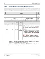
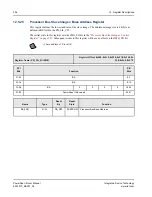
Register Name: P1_CONF_DATA
Register Offset: 0x148
PCI
Bits
Function
PB
Bits
31-24
CDATA
0-7
23-16
CDATA
8-15
15-08
CDATA
16-23
07-00
CDATA
24-31
Name
Type
Reset
By
Reset
State
Function
CDATA [31:0]
R/W
P1_RST
0
Configuration data


