12. Register Descriptions
280
PowerSpan II User Manual
80A1010_MA001_09
Integrated Device Technology
www.idt.com
12.5.18
PCI-1 to PCI-2 Interrupt Acknowledge Cycle Generation Register
Reading this register from the PCI-1 bus causes an IACK cycle to be generated on the PCI-2 Interface.
The byte lanes enabled on the PCI-2 bus are determined by P1_CBE#[3:0] of the PCI-1 Memory Read
cycle. The address on the PCI-1 bus used to access the P1_IACK register is passed directly over to the
PCI-2 bus during the PCI IACK cycle. However, address information is ignored during PCI IACK
cycles and has no effect.
Reads from this register behave as delayed transfers. This means that the PCI-1 bus master is retried
until the read data is latched from the PCI-2 target. When the IACK cycle completes on the PCI-2 bus,
the IACK_VEC[31:0] field is returned as read data when the PCI-1 bus master returns after the retry.
Writing to this register from the Processor Bus or either PCI bus has no effect. Reads from the PCI-2
Interface and Processor Bus return all zeros.
This register is not implemented in the Single PCI PowerSpan II and must be treated as reserved.
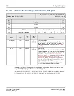
Register Name: P1_IACK
Register Offset: 0x14C
PCI
Bits
Function
PB
Bits
31-24
IACK_VEC
0-7
23-16
IACK_VEC
8-15
15-08
IACK_VEC
16-23
07-00
IACK_VEC
24-31
Name
Type
Reset
By
Reset
State
Function
IACK_VEC
[31:0]
R
P1_RST
0
PCI IACK Cycle Vector


