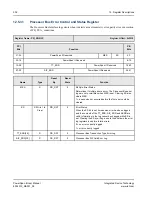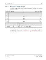
12. Register Descriptions
296
PowerSpan II User Manual
80A1010_MA001_09
Integrated Device Technology
www.idt.com
12.5.27
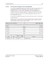
Processor Bus PCI Configuration Cycle Information Register
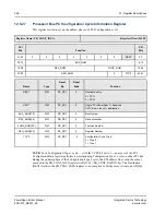
This register is used to set up the address phase of a PCI Configuration cycle.
TYPE:
For a Configuration Type 1 cycle
—
with the TYPE bit set to 1
—
an access of the PCI
Configuration Data register performs a corresponding Configuration Type 1 cycle on either PCI bus.
During the address phase of the Configuration Type 1 cycle, the PCI address lines carry the values
encoded in the PB_CONF_INFO register (AD[31:0] = PB_CONF_INFO[31:0]). The Destination
(DEST) field, in the PB_CONF_INFO register, is an exception to this because it is zero on AD[24].
Register Name: PB_CONF_INFO
Register Offset: 0x290
PCI
Bits
Function
PB
Bits
31-24
0
0
0
0
0
0
0
DEST
0-7
23-16
BUS_NUM
8-15
15-08
DEV_NUM
FUNC_NUM
16-23
07-00
REG_NUM
0
TYPE
24-31
Name
Type
Reset
By
Reset
State
Function
DEST
R/W
PB_RST
0
Destination Bus
0 = PCI 1
1 = PCI-2
DEST
R/W
PB_RST
0
Single PCI PowerSpan II: Reserved
PCI-1 Bus is the only destination.
BUS_NUM[7:0]
R/W
PB_RST
0
Bus Number
DEV_NUM[4:0]
R/W
PB_RST
0
Device Number
FUNC_NUM[2:0]
R/W
PB_RST
0
Function Number
REG_NUM[5:0]
R/W
PB_RST
0
Register Number
TYPE
R/W
PB_RST
0
Configuration Cycle Type
0 = Type 0
1 = Type 1


