12. Register Descriptions
307
PowerSpan II User Manual
80A1010_MA001_09
Integrated Device Technology
www.idt.com
12.5.34
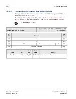
Processor Bus Arbiter Control Register
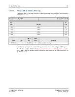
The arbitration control register is used to control the parameters of the on-chip Processor Bus arbiter.
Register Name: PB_ARB_CTRL
Register Offset: 0x2D0
PCI
Bits
Function
PPC
Bits
31-24
PowerSpan II Reserved
0-7
23-16
PowerSpan II Reserved
M3_EN
M2_EN
M1_EN
0
8-15
15-08
PowerSpan II Reserved
M3_PRI
M2_PRI
M1_PRI
PS_PRI
16-23
07-00
PowerSpan II Reserved
TS_DLY
PARK
BM_PARK
24-31
Name
Type
Reset
By
Reset
State
Function
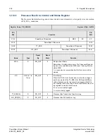
Mx_EN
R/W
PB_RST
PWRUP
External Master x Enable
When set, the arbiter recognizes address bus requests for
this master. When cleared, the arbiter ignores address bus
requests from this master (see
).
0=External requests ignored
1=External requests recognized
Mx_PRI
R/W
PB_RST
0
External Master x Priority Level
Determines the arbitration priority for external masters.
0 = Low Priority
1 = High Priority
PS_PRI
R/W
PB_RST
0
PowerSpan II Priority Level
0 = Low Priority
1 = High Priority
TS_DLY
R/W
PB_RST
0
Controls when arbiter samples requests
When set, the PB arbiter samples incoming requests two
clocks after a TS_ signal is received. When cleared, the
arbiter samples requests one clock after a TS_ signal is
received. The default state is 0.
An example application for this feature is some L2 caches
hold the BR_ signal after the TS_ signal starts. The
PowerSpan II arbiter could see this as a valid request and
give the bus to the L2 cache when the bus was not
requested. This bit delays when the PB arbiter samples the
signal so a false bus request is not granted.
0 = sample clock after TS_
1 = sample 2 clocks after TS_


