12. Register Descriptions
324
PowerSpan II User Manual
80A1010_MA001_09
Integrated Device Technology
www.idt.com
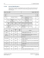
12.5.44
Reset Control and Status Register
This register contains the read-only bits that specify all PowerSpan II power-up options and status of a
number of pins that are normally fixed for each application.
Register Name: RST_CSR
Register Offset: 0x40C
PCI
Bits
Function
PB
Bits
31-24
PB_RST_
DIR
PB_ARB_
EN
PB_FAST
PCI_
BOOT
PowerSpan II Reserved
0-7
23-16
P1_RST_
DIR
P1_ARB_
EN
P1_M66
EN
PowerSpan II Reserved
P1_R64_
EN
P1_D64
8-15
15-08
P2_RST_
DIR
P2_ARB_
EN
P2_M66
EN
PowerSpan II Reserved
PRI_PCI
16-23
07-00
Power-Sp
an II Rsvd
7400_
MODE
BYPASS_
EN
ELOAD
PowerSpan II Reserved
24-31
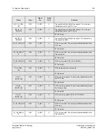
Name
Type
Reset
By
Reset
State
Function
PB_RST_DIR
R
G_RST
PWRUP
Status of PB_RST_DIR pin.
PB_ARB_EN
R
G_RST
PWRUP
Processor bus arbiter enable.
0=Disabled power-up option
1=Enabled power-up option
PB_FAST
R
G_RST
PWRUP
Processor Bus Clock Frequency Selection
Indicates the latched value of the PB_FAST pin. This bit is
used to optimally configure the Processor Bus Interface PLL
for the desired operating frequency.
0=25 MHz to 50 MHz
1=50 MHz to 100 MHz
PCI_BOOT
R
G_RST
PWRUP
PCI Boot
0=Boot from Processor Bus
1=Boot from PCI
P1_RST_DIR
R
G_RST
PWRUP
Status of P1_RST_DIR pin.
P1_ARB_EN
R
G_RST
PWRUP
PCI-1 arbiter enable
0=Disabled power-up option
1=Enabled power-up option


