12. Register Descriptions
325
PowerSpan II User Manual
80A1010_MA001_09
Integrated Device Technology
www.idt.com
P1_M66EN
R
G_RST
PWRUP
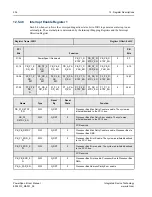
PCI-1 Clock Frequency Selection
Indicates the latched value of the P1_M66EN pin. This bit is
used to optimally configure the PCI-1 interface PLL for the
desired operating frequency.
0=25 MHz to 33 MHz
1=33 MHz to 66 MHz
P1_R64_EN
R
G_RST
PWRUP
P1_REQ64# output enable.
0=PowerSpan II does not assert P1_REQ64# at reset
1=PowerSpan II does assert P1_REQ64# at reset to indicate
the presence of a 64-bit P1_AD[] bus
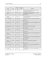
P1_D64
R
G_RST
PWRUP
PCI-1 Databus Width
Indicates the width of the databus to which the PCI-1
Interface is connected. This is determined by the level on
P1_REQ64# at the negation of P1_RST#, or by the level on
P1_64EN# (See
).
0=connected to 32-bit AD bus
1=connected to 64-bit AD bus
P2_RST_DIR
R
G_RST
PWRUP
Status of P2_RST_DIR pin.
Single PCI PowerSpan II: Reserved
P2_ARB_EN
R
G_RST
PWRUP
PCI-2 arbiter enable.
0=Disabled power-up option
1=Enabled power-up option
Single PCI PowerSpan II: Reserved
P2_M66EN
R
G_RST
PWRUP
PCI-2 Clock Frequency Selection
Indicates the latched value of the P2_M66EN pin. This bit is
used to optimally configure the PCI-2 interface PLL for the
desired operating frequency.
0=25 MHz to 50 MHz
1=33 MHz to 66 MHz
Single PCI PowerSpan II: Reserved
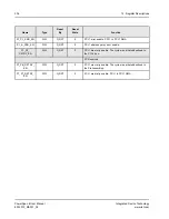
PRI_PCI
R
G_RST
PWRUP
Designated Primary PCI Bus.
0=PCI-1 is Primary
1=PCI-2 is Primary
Single PCI PowerSpan II: Reserved
Name
Type
Reset
By
Reset
State
Function


