12. Register Descriptions
334
PowerSpan II User Manual
80A1010_MA001_09
Integrated Device Technology
www.idt.com
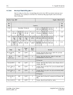
12.5.48
Interrupt Enable Register 1
Each bit, when set, allows the corresponding active status bit in ISR1 to generate an interrupt on an
external pin. The external pin is determined by the Interrupt Mapping Registers and the Interrupt
Direction Register.
Register Name: IER1
Register Offset: 0x41C
PCI
Bits
Function
PB
Bits
31-24
PowerSpan II Reserved
PB_P1_R
ETRY_EN
PB_P2_R
ETRY_EN
PB_PB_R
ETRY_EN
0
0-7
23-16
PB_P1_E
RR_EN
PB_P2_E
RR_
EN
PB_PB_E
RR_EN
PB_A_PA
R_EN
PB_P1_D
_PAR_EN
PB_P2_D
_PAR_EN
PB_PB_D
_PAR_EN
0
8-15
15-08
P2_P1_E
RR_
EN
P2_PB_E
RR_
EN
P2_P2_E
RR_
EN
P2_A_PA
R_EN
P2_P1_R
ETRY_EN
P2_PB_R
ETRY_EN
P2_P2_R
ETRY_EN
0
16-23
07-00
P1_P2_E
RR_
N
P1_PB_E
RR_EN
P1_P1_E
RR_EN
P1_A_PA
R_EN
P1_P2_R
ETRY_EN
P1_PB_R
ETRY_EN
P1_P1_R
ETRY_EN
0
24-31
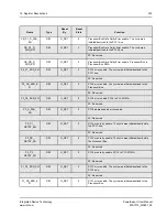
Name
Type
Reset
By
Reset
State
Function
PB_P1_RETRY_
EN
R/W
G_RST
0
Processor Bus Max Retry Counter enable. The cycle was
initiated/destined to the PCI-1 bus.
PB_P2_
RETRY_EN
R/W
G_RST
0
Processor Bus Max Retry Error enable. The cycle was
initiated/destined to the PCI-2 bus.
2P: Reserved
PB_PB_RETRY
R/W
G_RST
0
Processor Bus Max Retry Counter enable. Processor Bus to
Processor Bus DMA.
PB_P1_ERR_E
N
R/W
G_RST
0
Processor Bus Error Enable. The cycle was initiated/destined
to the PCI-1 bus.
PB_P2_ERR_E
N
R/W
G_RST
0
Processor Bus Error enable. The cycle was initiated/destined
to the PCI-2 bus.
2P: Reserved
PB_PB_ERR_E
N
R/W
G_RST
0
Processor Bus Error enable. Processor Bus to Processor Bus
DMA.
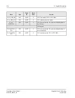
PB_A_PAR_EN
R/W
G_RST
0
Processor Bus Address Parity Error enable


