15. AC Timing
408
PowerSpan II User Manual
80A1010_MA001_09
Integrated Device Technology
www.idt.com
15.4
Timing Diagrams
The timing diagrams in this section apply to both the Single PCI PowerSpan II and the Dual PCI
PowerSpan II.
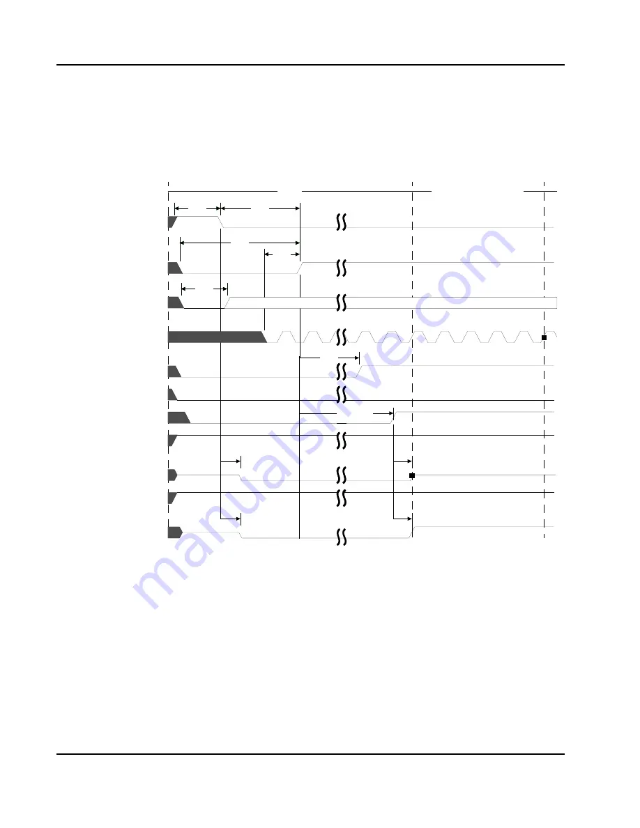
Figure 30: Power-up Reset: CompactPCI Adapter Scenario
Notes:
1.
P1_RST# configured as input
2.
PB_RST_ and P2_RST# configured as output
3.
If JTAG is not used, the TRST_ signal can be pulled low through a resistor (~2.5 KOhm).
Reset
Ready for initialization
t104
t104
t104
t104
t103
t428
t428
t102
t100
t100
t101
t100
t100
HEALTHY_
PO_RST_
TRST_
Px_CLK
plls locked
P1_RST_DIR
P1_RST#
PB_RST_DIR
PB_RST_
P2_RST_DIR
P2_RST#
t105


