A. Hardware Implementation
418
PowerSpan II User Manual
80A1010_MA001_09
Integrated Device Technology
www.idt.com
A.3
PLL External Decoupling
The PLLs in the PowerSpan II device should be externally decoupled in order to have the cleanest
possible supply environment. IDT recommends two decoupling scenarios for PowerSpan II. The first
recommendation is a backwards compatible design that enables migrating PowerSpan II users to
employ the decoupling scheme used in the original PowerSpan II. The second recommendation is for
new PowerSpan II designs.
A.3.1
Backwards Compatible PLL Decoupling for Migrating PowerSpan II
Designs
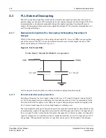
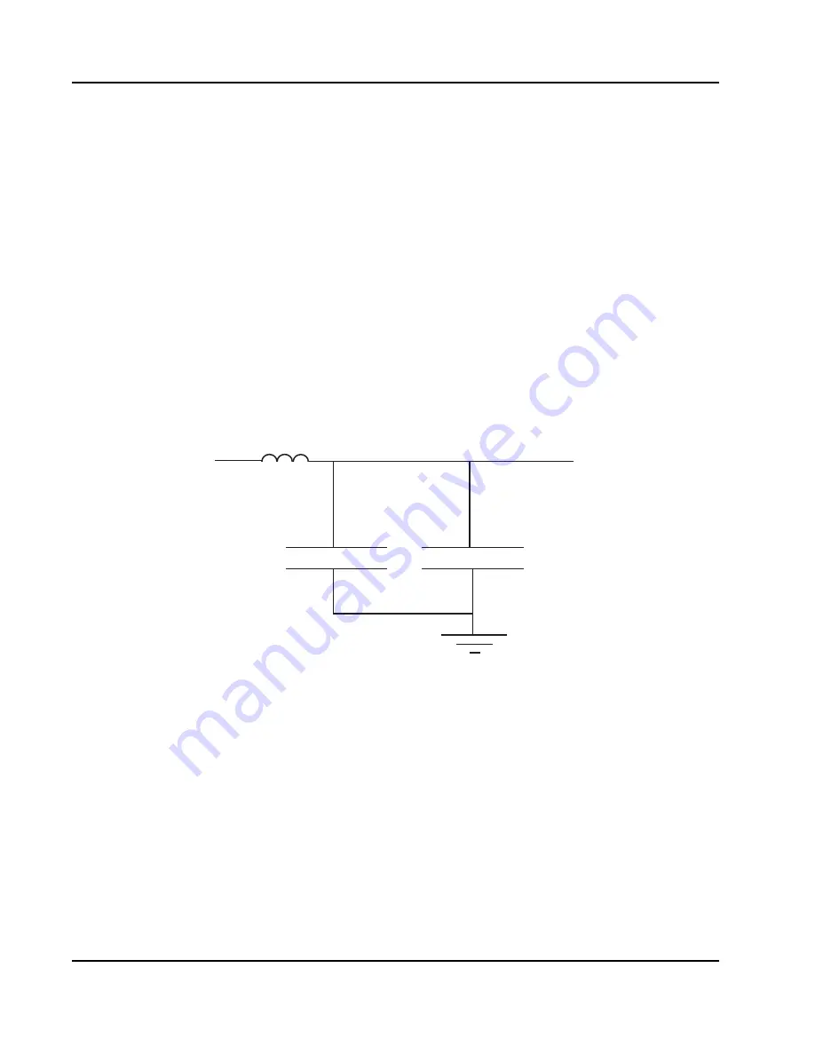
VDDA is the voltage supply pin to the analog circuits in the PLL. Noise on VDDA can cause phase
jitter at the output of the PLL. To provide isolation from the noisy internal digital circuitry, a filter
circuit can be placed on VDDA (see
).
Figure 41: PLL Power Filter
All wire lengths must be kept short in order to minimize coupling from other signals.
A.3.1.1
Recommended Decoupling Capacitors
PowerSpan II requires the Core Supply Voltage (Vdd Core (2.5V)) and I/O Supply Voltage (Vdd I/O
(3.3V)) be decoupled to reduce switching noise. One bulk capacitor of 10 uF is recommended for the
Vdd Core and Vdd I/O supplies. Every third pair of power and ground pins must be decoupled with a
0.1 uF surface mount capacitor to reduce high frequency switching noise.
The track lengths from the power and ground pins to the capacitors must be kept as short. Based on this
recommendation, eight 0.1uF capacitors are required for the I/O supply and twelve 0.1uF capacitors for
the core supply. In order to keep the track lengths to the capacitors as short as possible, use integrated
capacitor components. It is possible to obtain components which have four 0.1uF capacitors in a 0612
size package. Other quantities and values of capacitors can be used at the discretion of the designer.
VDD
VDDA
C = 0.1
μ
F
C= 1
μ
F
Ferrite Bead = Murata BLM32A06 or equivalent
+


