10. Endian Mapping
185
PowerSpan II User Manual
80A1010_MA001_09
Integrated Device Technology
www.idt.com
10.4.2
Little-endian Mode
When operating in little-endian mode, PowerSpan II uses a data invariant scheme for mapping
PowerPC byte lanes. Data invariance preserves the relative byte significance of a structure in both PCI
and PowerPC spaces, but translates the byte addressing.
In order to access PCI device registers from the processor bus in little-endian mode, there are certain
addressing rules which must be followed. In PowerSpan II when little-endian mode is selected, no
address swapping takes place (refer to
). This means that the MSB on the
processor bus goes to the MSB on PCI. However, the MSB on processor bus is the low address and
MSB on PCI is the high address.
10.4.2.1
4 Byte Transactions
When performing 4 byte transactions to the PCI bus in little-endian mode the intended address must
XOR the address with 0x4. This creates the address for PCI which is used in the transaction.
In little-endian mode for 4 byte transfers, the following changes must be made:
•
Change a register on PCI at offset 0x0 using address 0x4
•
Change a register on PCI at offset 0x4 using address 0x0
•
Change a register on PCI at offset 0x8 using address 0xC
•
Change a register on PCI at offset 0xC using address 0x8
These rules enable the transactions to reach the intended targets without manual code changes.
PowerSpan II byte lane mappings for little-endian mode support are illustrated in
.
Seven
bytes
000
D0
D1
D2
D3
D4
D5
D6
D6
D5
D4
D3
D2
D1
D0
001
D1
D2
D3
D4
D5
D6
D7
D7
D6
D5
D4
D3
D2
D1
Double
000
D0
D1
D2
D3
D4
D5
D6
D7
D7
D6
D5
D4
D3
D2
D1
D0
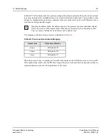
Table 51: PowerSpan II Big-endian Mode Byte Lane Mapping
Transfer
Size
Start
Address
PowerPC Byte Lanes
PCI Byte Lanes
0
1
2
3
4
5
6
7
7
6
5
4
3
2
1
0


