12. Register Descriptions
292
PowerSpan II User Manual
80A1010_MA001_09
Integrated Device Technology
www.idt.com
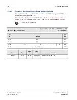
12.5.24
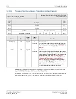
Processor Bus Slave Image x Translation Address Register
TADDR
: The Translation Address register replaces the Processor Bus address, up to the size of the
image. TADDR[31:12] replace the Processor Bus PB_A[0:19].
For example, if TADDR[31:12] = 0x12345 and PB_SIx_CTL[BS]=0 (4 K image) and the address on
the Processor Bus is PB_A[0:31] = 0x78563412, then the PCI address becomes 0x12345412
Register Name: PB_SIx_TADDR
Register Offset: 0x204, 0x214, 0x224, 0x234, 0x244,
0x254, 0x264, 0x274
PCI
Bits
Function
PB
Bits
31-24
TADDR
0-7
23-16
TADDR
8-15
15-08
TADDR
PowerSpan II Reserved
16-23
07-00
PowerSpan II Reserved
M3
M2
M1
0
24-31
Name
Type
Reset
By
Reset
State
Function
TADDR[19:0]
R/W
PB_RST
0
EEPROM
Translation Address
The Translation Address register replaces the Processor
Bus address, up to the size of the image. TADDR[31:12]
replace the Processor Bus PB_A[0:19] (see
).
M3-M1
R/W
PB_RST
0
EEPROM
Master Select
These bits indicate which external master(s) are qualified
to access the image. The image supports master decode if
the Processor Bus arbiter is enabled — the Processor Bus
Arbiter Enable bit, in the
, is set and when MD_EN bit in the
“Processor Bus Slave Image x Control Register” on
page 287
is set. Bit M3 represents the external master
connected to PB_BG[3]_ and M1 represents the external
master connected to PB_BG[1]_.
0=Do not claim transactions generated by this master
1=Claim transactions generated by this master


