12. Register Descriptions
322
PowerSpan II User Manual
80A1010_MA001_09
Integrated Device Technology
www.idt.com
12.5.43
I
2
C/EEPROM Interface Control and Status Register
This register supports the PowerSpan II I
2
C/EEPROM interface.
An I
2
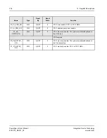
C bus cycle is initiated by writing to this register. Software must wait for the ACT bit to be zero
before starting a new I
2
C cycle. When the ACT bit is 1, writes to this register have no effect and the
DATA field is undefined.
The PCI VPD EEPROM Chip Select (VPD_CS) bit, in the
“Miscellaneous Control and Status
, selects the EEPROM where VPD resides. If VPD_CS is 000b, then VPD starts
at address offset 0x40 of the first EEPROM. For all other values of VPD_CS, VPD starts at address
offset 0x00 of the specified EEPROM.
Both the ACT bit and the ERR bit are updated five PB clocks after a PB write
completion (PB_TA asserted)
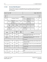
Register Name: I2C_CSR
Register Offset: 0x408
PCI
Bits
Function
PB
Bits
31-24
ADDR
0-7
23-16
DATA
8-15
15-08
DEV_CODE
CS
RW
16-23
07-00
ACT
ERR
PowerSpan II Reserved
24-31
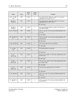
Name
Type
Reset
By
Reset
State
Function
ADDR[7:0]
R/W
G_RST
0
Specifies I
2
C device address to be accessed.
DATA[7:0]
R/W
G_RST
0
Specifies the required data for a write. Holds the data at
the end of a read.
DEV_CODE[3:0]
R/W
G_RST
1010
Device select. I
2
C 4-bit device code.
CS[2:0]
R/W
G_RST
0
Chip Select
RW
R/W
G_RST
0
0=read
1=write


