background image

Industrial Electronic Engineers, Inc.

SIZE

A

CODE IDENT

NO.

05464

S03858–06–0105

Van Nuys, California

Scale:  NONE

Rev   C

Sheet 15

4.5

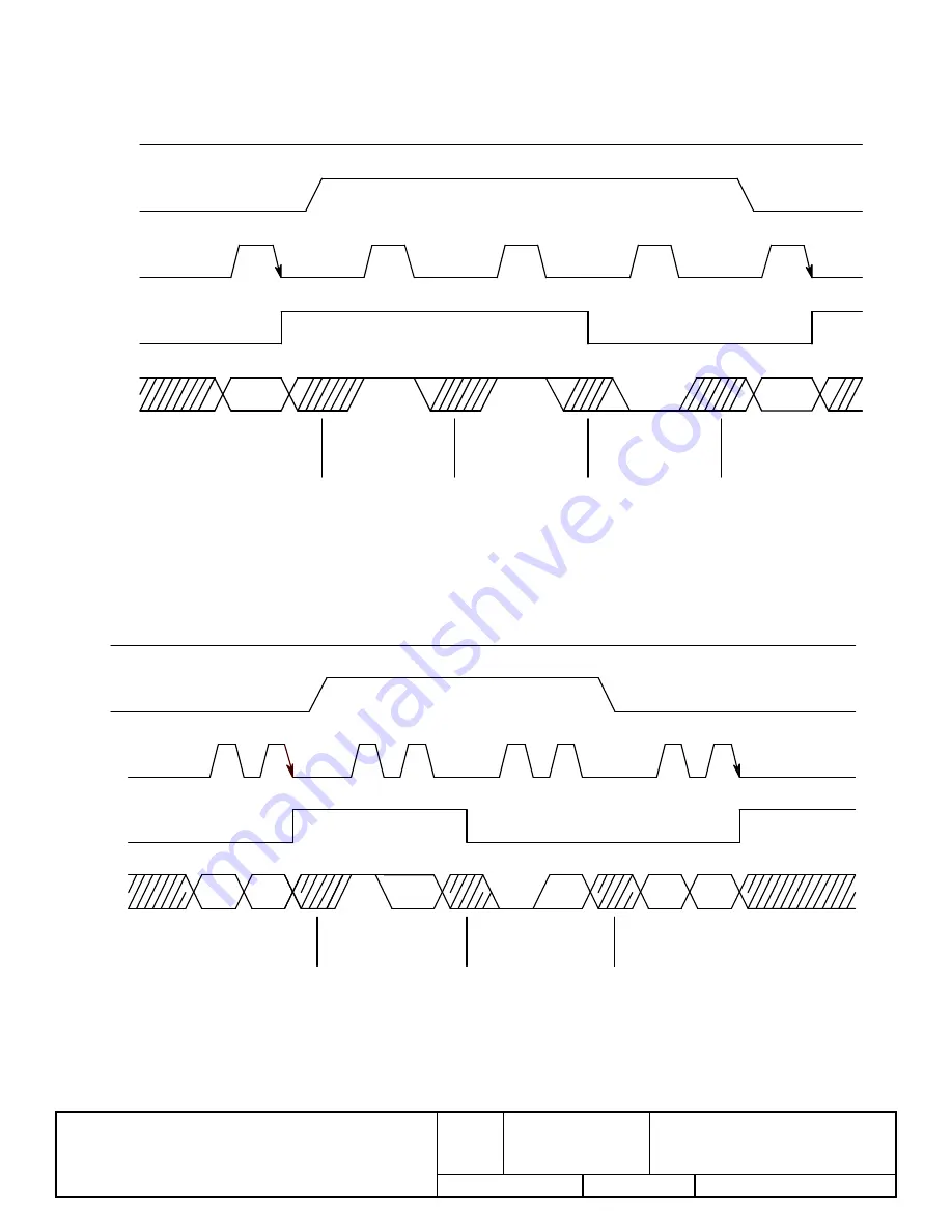
Timing Sequence for 8 Bit Parallel Interface

Figure 13 illustrates the typical Busy Flag check sequence for an 8 bit data interface.

Figure 13

Busy Flag Check Sequence for 8–bit Parallel Interface

4.6

Timing Sequence for 4 Bit Parallel Interface

Figure 14 illustrates the typical Busy Flag check sequence for a 4 bit data bus interface.

Figure 14

Busy Flag Check Sequence for 4–bit Parallel Interface

Note: IR

7

, IR

3

:

Instruction, 7th bit & 3rd bit

AC

3

:

Address Counter, 3rd bit

Data

Busy

Busy

IR 7

Not

Busy

Internal Operation

Instruction

Write

Instruction

Write

Busy Flag

Check

Busy Flag

Check

Busy Flag

Check

DB7

Internal

E

R/W

RS

DB

IR

7

IR

7

IR

3

AC

3

D

3

AC

3

Busy

Not

Busy

7

Internal Operation

E

RS

Instruction

Write

Busy Flag

Check

Busy Flag

Check

Instruction

Write

Summary of Contents for 03858-06-0105

Page 1: ...1 2 3 4 5 6 7 8 9 10 11 12 13 14 15 16 17 18 19 20 21 22 23 24 REVISION STATUS PROJ NO 411 CONTRACT INDUSTRIAL ELECTRONIC ENGINEERS INC VAN NUYS CALIFORNIA DRAWN R January 3 19 93 PARALLEL DATA INPUT...

Page 2: ...9 3 0 OPERATION 9 3 1 Instruction Set 9 3 2 Power Up Instructions Sequence 9 3 3 Instructions Affecting the Relationship of Display Position Cursor and DD RAM Address 9 3 4 Instructions Affecting Cus...

Page 3: ...7 3 Operation 9 7 3 1 Normal Operation 9 7 3 2 Brightness Voltage and Frequency Characteristics 9 7 3 3 Intermittent Operation 9 7 3 4 Square Waveform Operation 9 7 3 5 Operating Temperature 9 7 3 6 O...

Page 4: ...Conditions 9 Figure 9 Load Character with S 1 I D 0 from Initial Conditions 9 Figure 10 Load Character with S 1 I D 1 from Initial Conditions 9 Figure 11 Interface Timing Write Error Bookmark not defi...

Page 5: ...ons where the display is remotely located up to 50 feet from the host processor the serial data input option should be used The serial option model is described in IEE specification S03858 06 0205 1 3...

Page 6: ...work optimizes both viewing and contrast ratio for the display over all operating temperatures E RS R W DB 7 DB 4 DB DB 3 0 LCD Controller LCD Row Drivers and Shift Registers LCD Column Drivers and Sh...

Page 7: ...Seg40 Com1 Com16 D 5 5 40 Figure 2 LCD Controller Block Diagram 2 2 1 Instruction Register IR The IR stores instruction codes such as display clear and cursor shift and address information of the disp...

Page 8: ...nd Cursor or Display Shift instructions 2 2 6 Character Generator ROM CG ROM The CG ROM generates character patterns of 5 X 7 dots from 8 bit character codes The 192 5 X 7 dot matrix characters are il...

Page 9: ...ny bytes not used for character pattern information can be used for general purpose data RAM The 5 6 and 7 bits are never used for character pattern information and are always available for use 2 The...

Page 10: ...L Moves cursor or shifts entire display one position DD RAM contents are unchanged 40 s Function Set 0 0 0 0 1 DL 1 0 Sets Interface Data Length 40 s Set CG RAM Address 0 0 0 1 Sets CG RAM address CG...

Page 11: ...of DL I D S D C and B Don t care 3 3 Instructions Affecting the Relationship of Display Position Cursor and DD RAM Address The DD RAM contains the 8 bit character codes of the 40 characters displayed...

Page 12: ...07 08 09 0D 0E 0F 10 11 12 67 40 41 42 43 44 45 46 47 48 49 4D 4E 4F 50 51 52 13 14 15 16 17 18 19 1A 1B 1C 1D 21 22 23 24 25 26 53 54 55 56 57 58 59 5A 5B 5C 5D 61 62 63 64 65 66 Cursor Last Charact...

Page 13: ...to VCC 0 001 mA Supply Current logic ICC 6 12 mA Supply Current EL Lamp IBL VBL 5 VDC 120 mA 4 4 Timing Characteristics Write Operation Refer to Figure 11 Item Symbol Min Max Unit Enable Cycle Time t...

Page 14: ...rite Figure 12 Interface Timing Read Valid Data t t AS PWEH tAH tAH DSW t t H t V IL1 VIL1 VIL1 V IL1 VIL1 VIL1 VIL1 V IH1 VIH1 VIH1 VIH1 V IH1 VIL1 RS R W E DB 0 7 DB cyc t t t t t t tEf t t t t t t...

Page 15: ...for 4 Bit Parallel Interface Figure 14 illustrates the typical Busy Flag check sequence for a 4 bit data bus interface Figure 14 Busy Flag Check Sequence for 4 bit Parallel Interface Note IR7 IR3 Inst...

Page 16: ...Ground 11 DB0 12 Ground 13 DB1 14 Ground 15 DB2 16 Ground 17 DB3 18 Ground 19 DB4 20 Ground 21 DB5 22 VCC 5VDC Parallel with Pin 24 23 DB6 24 VCC 5VDC Parallel with Pin 22 25 DB7 26 N C When the displ...

Page 17: ...TIONS 6 1 Optical Characteristics Format Four lines of 20 characters Character Font 5x7 dot matrix with cursor Character Height w cursor 0 48 12 1mm Character Height w o cursor 0 39 9 9mm Character Wi...

Page 18: ...90 Figure 15 Definition of Vertical Viewing Angle Definition of Horizontal Viewing Angle top Viewing Display for Bottom Viewing Displays 20 Typically X X Y Y Normal 20 90 90 Figure 16 Definition of Ho...

Page 19: ...rd potentiometer This is considered to be a nominal adjustment but the user may prefer to vary this to optimize the viewing for a particular application The bias voltage is measured between VCC pin 22...

Page 20: ...typical operation at 90 Volts AC at 330 cycles The light output of the lamp under these operating conditions is typically 12 ft L Since the LCD transmits approximately 8 of the light the light output...

Page 21: ...cy components in the square wave as distance from the bus bar increases Consequently the waveform is rounded at distances away from the bus bar Second the leading edge of a square wave contains high o...

Page 22: ...Figure 21 Brightness vs Time 7 4 Electromagnetic Interference EMI Electroluminescent lamps have been shown to radiate negligible interference through UHF when operated by quasi sinusoidal waveforms 7...

Page 23: ...d between the window material and the surface of the LCD to prevent the transfer of static charges to the front surface of the LCD Supertwist LCD s may activate un driven elements in response to a sur...

Page 24: ...ustrial Electronic Engineers Inc SIZE A CODE IDENT NO 05464 S03858 06 0105 Van Nuys California Scale NONE Rev C Sheet 24 10 0 OUTLINE AND MOUNTING CHARACTERISTICS Figure 22 03858 06 0105 Outline Drawi...

Reviews: