Industrial Electronic Engineers, Inc.
SIZE
A
CODE IDENT NO.
05464
S03858–21–0205
Van Nuys, California
SCALE N/A
REV B
SHEET 18
4.0
INTERFACE AND CONTROL
4.1
Connector Assignment (P2)
Pin No.
Function
P2–1
R
X
Data
P2–2
R
X
Data RTN (Signal Ground)
P2–3
RESET
P2–4
Adjust
P2–5
Self–Test
P2–6
V
BIAS
(Factory Test Point)
P2–7
V
CC
(+5 Volts)
P2–8
V
SS
(Ground)
P2–9
No Connection
P2–10
Optional Backlight
P2–11
Optional Backlight
4.2
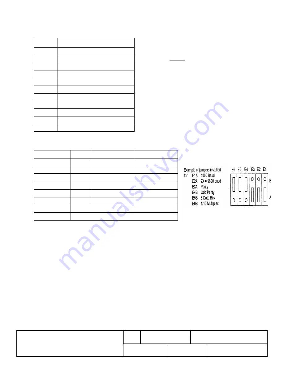
Jumper Settings
Jumper No.
Pins
Jumper A = “0”
Jumper B = “1”
1
E1
4800 Baud
1200 Baud
2
E2
2 x Baud
1 x Baud
3
E3
Parity
No Parity
♦
4
E4
Even Parity
Odd Parity
5
E5
7 Data Bits ***
8 Data Bits
6
E6
1/8 Mpx (N/A)
1/16 Mpx
7**
Not Used
8**
Not Used
*
Baud rate will default to "1" if no jumper is installed.
**
Jumper options 7, and 8 are omitted and will indicate as logic "1" when in self–test mode.
***
8 bit word preferred. When 7 bit word is selected see section 3.1.2 for use of instruction 19 Hex.
♦
Selection of NO PARITY requires use of two stop bits.
5.0
ELECTRICAL SPECIFICATIONS
5.1
Absolute Maximum Ratings
Power Supply Voltage (V
CC
):
–0.3 to +6.5 V
DC
Serial Input Voltage:
–25.0 to +25.0 V
DC
5.2
Normal Operating Ratings
Power Supply Voltage (V
CC
):
+5.0 V
DC
±10%
Power Supply Current:
34 mA Max
Backlight Current (+5 Volt Inverter): 100 mA
NOTE: The mating connector
must be wired in a reverse pin
sequence from its marking. (Pin
11 is Pin 1 etc.)
The mating connector is a Molex
#22-01-2117 or equivalent. It uses
crimp pins #08-50-0114.

