background image

Industrial Electronic Engineers, Inc.

SIZE

A

CODE IDENT NO.

05464

S03858–21–0205

Van Nuys, California

SCALE     N/A

REV  B

SHEET  9

2.2.7

Character Generator RAM (CG RAM)

The CG RAM allows the user to define 8 types of 5 X 7 character patterns.  Figure 4 shows the relationship
between CG RAM addresses and data patterns (Refer to Set CG RAM Address and Write to CG or DD RAM
instructions).

Character Codes

(DD RAM Data)

CG RAM

Address

Character Patterns

(CG RAM Data)

7

6

5

4

3

2

1

0

5

4

3

2

1

0

7

6

5

4

3

2

1

0

Higher Order Bits

Lower Order Bits

Higher Order Bits

Lower Order Bits

Higher Order Bits

Lower Order Bits

0

0

0

*

*

*

1

1

1

1

0

0

0

1

1

0

0

0

1

0

1

0

1

0

0

0

1

Character

0

1

1

1

1

1

1

0

Pattern

0

0

0

0

*

0

0

0

0

0

0

1

0

0

1

0

1

0

0

Example

1

0

1

1

0

0

1

0

1

1

0

1

0

0

0

1

1

1

1

*

*

*

0

0

0

0

0

Cursor

Figure 4 Relationship Between CG RAM Address, Character Codes (DD RAM)

and Character Patterns (CG RAM Data)

NOTES:

1)  The CG RAM consists of 64 bytes.  Any bytes not used for character pattern information can be

used for general purpose data RAM.  The 5, 6 and 7 bits are never used for character pattern
information and are always available for use.

2)  The 0, 1 and 2 bits of character code correspond to the 3, 4 and 5 bits of the CG RAM address.

3)  The 0, 1 and 2 bits of the CG RAM address specify the row of the character pattern.

4)  The 8th row of the character pattern corresponds to the cursor character pattern.  If any bit in the

row is "1", then the corresponding cursor bit is a "1" regardless of cursor position.  (For most
applications, the data should be "0" in this row, which allows for normal cursor operation on the
character.)

5)  Since bit 3 is a "don't care", two character codes represent the same special character.  For

example, a character code of 07 (hexadecimal) selects the same character pattern as OF
(hexadecimal).

2.2.8

Parallel/Serial Data Conversion Circuitry, Timing Generator Circuitry

These blocks control the interface to the LCD drivers.

Summary of Contents for 03858-21-0205

Page 1: ... B B B B B B B B B B B B B SHEET 1 2 3 4 5 6 7 8 9 10 11 12 13 14 15 16 17 18 19 20 21 22 23 24 REVISION STATUS PROJ NO 411 CONTRACT INDUSTRIAL ELECTRONIC ENGINEERS INC VAN NUYS CALIFORNIA DRAWN R January 3 19 93 SERIAL DATA INPUT CHECK 4 X 40 LCD MODULE WITH EL BACKLIGHT NOTICE IS HEREBY GIVEN THAT THIS DRAWING IS PART OF A PROPRIETARY ITEM OWNED BY INDUSTRIAL APPROVED SIZE CODE IDENT NO ELECTRON...

Page 2: ...M CG RAM 9 2 2 8 Parallel Serial Data Conversion Circuitry Timing Generator Circuitry 9 3 0 THEORY OF OPERATION 10 3 1 Serial Interface 10 3 2 Error Detection and Reporting 10 3 3 Power up Sequence 11 3 4 Transmission Sequence for Instructions 11 3 5 Instruction Set 12 3 5 1 Instruction Summary 13 3 5 2 Sample Instructions In BASIC 13 3 6 Down Loadable Special Characters 14 3 7 Self test 16 3 8 Di...

Page 3: ... 1 EL Backlight Description 22 8 2 Electrical Characteristics of EL Backlight 22 8 3 Operation 22 8 3 1 Normal Operation 22 8 3 2 Operating Temperature 22 8 3 2 Brightness Voltage and Frequency Characteristics Continued 23 8 3 3 Intermittent Operation 23 8 3 4 Square Waveform Operation 23 8 3 5 Operating Temperature 23 8 3 6 Operating Life 23 8 4 Electromagnetic Interference EMI 24 8 5 DC AC Inver...

Page 4: ...ial Data Format 10 Figure 6 Default Configuration at Power up 11 Figure 7 Instruction Sequence 11 Figure 8 Data Sequence 11 Figure 9 Instruction Set 12 Figure 10 Down loadable Special Characters 15 Figure 11 Power Supply Requirements 18 Figure 12 External Reset Circuit 18 Figure 13 Definition of Vertical Viewing Angle 20 Figure 14 Definition of Horizontal Viewing Angle 20 Figure 15 Definition of C...

Page 5: ...stics of the new Super Bi refringent Effect SBE liquid crystal cell used in this display The serial data input model of the 03858 21 Daystar Nova display allows communication between a host processor and the display by means of a serial RS 232C interface This provides the capability to communicate over a longer distance than is possible with the parallel model The RS 232 interface is a two wire co...

Page 6: ...e the function All three inputs may be left open if not used The VBIAS test point is used at the factory to preset the viewing angle The LCD Controllers are microprocessor units MPU designed specifically to control all multiplexing and character decoding functions for the LCD display LCD Controller 1 LCD Cell Column Drivers LCD Controller 2 Column Drivers Microprocessor Temperature Compensation 3 ...

Page 7: ...Seg1 Seg40 Com1 Com16 D 5 5 40 Figure 2 LCD Controller Block Diagram 2 2 1 Instruction Register IR The IR stores instruction codes such as display clear and cursor shift and address information of the display data RAM DD RAM and character generator RAM CG RAM The IR can be written from the MPU but not read 2 2 2 Data Register DR The DR temporarily stores data to be written into or read from the DD...

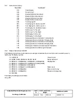
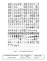
Page 8: ...OM CG ROM The CG ROM generates character patterns of 5 X 7 dots from 8 bit character codes The 192 5 X 7 dot matrix characters are illustrated in Figure 3 Figure 3 Correspondence Between Character Codes and Character Patterns Note Addresses 00h through 0Fh are reserved for CG RAM Addressing Addresses 10h through 1Fh and 80h through 9Fh are not used ...

Page 9: ...haracter Patterns CG RAM Data NOTES 1 The CG RAM consists of 64 bytes Any bytes not used for character pattern information can be used for general purpose data RAM The 5 6 and 7 bits are never used for character pattern information and are always available for use 2 The 0 1 and 2 bits of character code correspond to the 3 4 and 5 bits of the CG RAM address 3 The 0 1 and 2 bits of the CG RAM addres...

Page 10: ...no parity and two stop bits Since two command characters and numerous data characters are 8 bits in length it is recommended to operate in 8 bit mode if the host has this capability Where this is not possible 7 bit mode should be jumper selected see section 4 2 and a special command character 19h must be sent prior to each 8 bit command or data character i e characters where B7 1 Figure 5 represen...

Page 11: ... Jumper defined per section 4 2 Parity bit present Parity checking enable Parity Odd or Even 7 or 8 data bits Multiplex rate of LCD Display clear YES Display ON OFF ON Cursor location Position 0 Cursor OFF Entry mode set Shift cursor right after character entry Controller 1 Data Instructions Data Figure 6 Default Configuration at Power up 3 4 Transmission Sequence for Instructions Figures 7 and 8 ...

Page 12: ...Sets DD RAM address DD RAM data is sent or received after this is set 40µs Read Busy Flag and Address BF Reads Busy Flag BF and Address Counter 0µs Write Data to CG or DD RAM Writes data into CG RAM or DD RAM 40µs Read Data from CG or DD RAM Reads data from CG RAM or DD RAM 40µs Controller 1 Instructions 0 0 0 1 0 0 0 1 Subsequent data is Display Module Instructions for controller 1 Controller 1 D...

Page 13: ... Electronic Engineers Inc SIZE A CODE IDENT NO 05464 S03858 21 0205 Van Nuys California SCALE N A REV B SHEET 13 DL 0 4 bit operation BF 1 Operating internally BF 0 Can accept instruction Figure 9 Instruction Set ...

Page 14: ...ler 1 Instruction S 12h Subsequent Data Is Controller 1 Display Data 15h Subsequent Data Is Controller 2 Instruction S 16h Subsequent Data Is Controller 2 Display Data 17h Subsequent Data Down Loads Special Characters 19h Subsequent Data Is 8 Bit Length Character 3 5 2 Sample Instructions In BASIC The following instructions are provided as an example to illustrate the correct form and to assist th...

Page 15: ... as described in section 4 4 the user has these additional preformatted characters available Note that all down loaded character data is lost and must be reloaded after power has been removed To facilitate the use of these characters a subsequent data instruction 17h is used to inform the microprocessor that the following two bytes of data identify 1 the location of the special character to be dow...

Page 16: ...Industrial Electronic Engineers Inc SIZE A CODE IDENT NO 05464 S03858 21 0205 Van Nuys California SCALE N A REV B SHEET 16 Figure 10 Down loadable Special Characters ...

Page 17: ...bit settings 3 8 Diagnostics 1 The display module can be operated by the host in a HEX dump mode This diagnostic mode provides for the HEX display of all serial data received While operating in this mode the module will ignore the multiplex jumper setting and operate the display in a 1 8 multiplex mode 2 Check the module jumpers for proper baud speed and parity settings Section 4 2 3 With power OF...

Page 18: ...1 8 Mpx N A 1 16 Mpx 7 Not Used 8 Not Used Baud rate will default to 1 if no jumper is installed Jumper options 7 and 8 are omitted and will indicate as logic 1 when in self test mode 8 bit word preferred When 7 bit word is selected see section 3 1 2 for use of instruction 19 Hex Selection of NO PARITY requires use of two stop bits 5 0 ELECTRICAL SPECIFICATIONS 5 1 Absolute Maximum Ratings Power S...

Page 19: ...Requirements To utilize the optional external reset the RESET pin must be held at ground 0 5 Volts for at least 10 milliseconds after the power supply is within the voltage tolerance Figure 12 shows the module Reset circuit 5V 1k 3 3k 330 1uF Microprocessor Internal Pull down J2 Pin 3 Figure 12 External Reset Circuit 5 3 Interface Signals 5 3 1 Serial Interface Signals The display is designed to b...

Page 20: ...NS 7 1 Optical Characteristics Format Four lines of 40 characters Character Font 5x7 dot matrix with cursor Character Height w cursor 0 48 12 1mm Character Height w o cursor 0 39 9 9mm Character Width 0 24 6 1mm Overall Active Area 5 70 x 2 34 144 9mm x 59 5mm Peak Vertical Viewing Angle 20 below normal plane Viewing Mode Transflective light field Item Symbol Condition Min Typ Max Unit Viewing Ang...

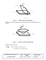
Page 21: ...Figure 13 Definition of Vertical Viewing Angle Definition of Horizontal Viewing Angle top Viewing Display for Bottom Viewing Displays φ 20 Typically X X Y Y Normal φ 20º θ θ θ 90º θ 90º Figure 14 Definition of Horizontal Viewing Angle Display contrast ratio is given by CR B B 2 1 Where B1 Brightness of selected segment B2 Brightness of non selected segment ...

Page 22: ...oard potentiometer This is considered to be a nominal adjustment but the user may prefer to vary this to optimize the viewing for a particular application The bias voltage is measured between VCC pin 7 and VBIAS pin 6 The viewing angle and contrast ratio may be externally controlled using an additional 10K ohm potentiometer The potentiometer on the rear of the module must first be set to the maxim...

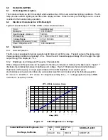
Page 23: ...pical operation at 90 Volts AC at 330 cycles The light output of the lamp under these operating conditions is typically 12 ft L Since the LCD transmits approximately 8 of the light the light output through the display is 1 ft L 8 3 2 Brightness and Voltage and Frequency Characteristics Other voltages and frequencies can be applied to the lamp to increase or decrease the light output Figure 17 illu...

Page 24: ...e bus bar increases Consequently the waveform is rounded at distances away from the bus bar Second the leading edge of a square wave contains high order harmonics which may cause radio interference EMI 8 3 5 Operating Temperature The maximum continuous operating temperature for the EL backlight is specified at 40 C Service may be extended to 70 C at a sacrifice in life At temperatures above 70 C a...

Page 25: ...ant power mode which provides for long lifetime at a relative constant light output Because of the quasi sinusoidal output RFI is minimal and usually no shielding is required 9 0 INSTALLATION NOTE To protect the front polarizer from accidental damage it is highly recommended that the LCD be mounted behind a clear glass or polycarbonate window material It is also recommended that an air gap of at l...

Page 26: ...ustrial Electronic Engineers Inc SIZE A CODE IDENT NO 05464 S03858 21 0205 Van Nuys California SCALE N A REV B SHEET 26 11 0 OUTLINE AND INSTALLATION CHARACTERISTICS Figure 20 03858 21 0205 Outline Drawing ...

Reviews: