background image

Industrial Electronic Engineers, Inc.

SIZE

A

CODE IDENT

NO.

05464

S03875–06–0114

Van Nuys, California

Scale:  NONE

Rev  A

Sheet 6

2.0

LOGICAL STRUCTURE AND FUNCTION

2.1

LCD Module

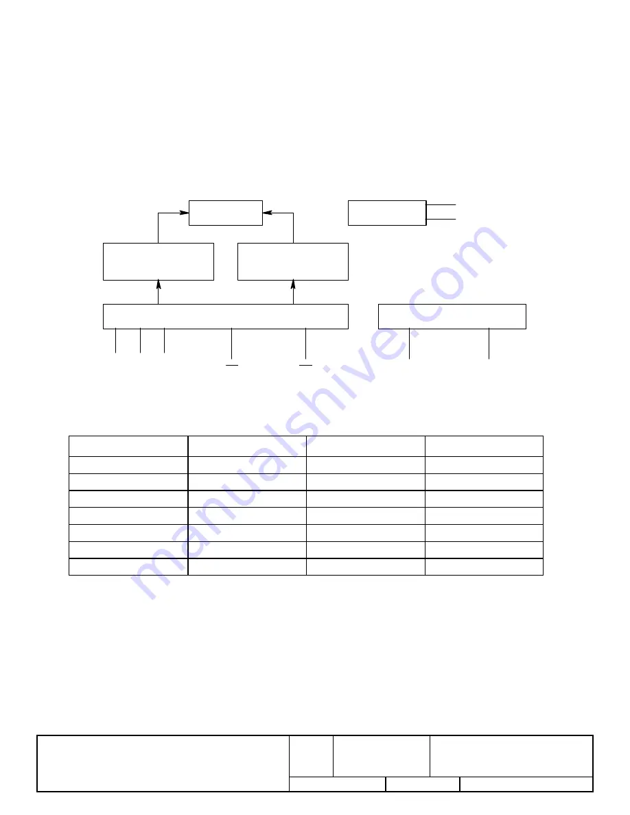
Figure 1 illustrates the major components of the serial option Daystar Nova module.  The module provides
means for an external viewing angle adjustment potentiometer (V

BIAS

 Adj.) at Pin 4, and connections for optional

RESET and self–test switches at Pins 3 and 5.  The external viewing angle adjustment potentiometer should be
connected to the same +5 Volt supply as the display module.  RESET and TEST pull down to ground to
activate the function.  All three inputs may be left open if not used.  The V

BIAS

 test point is used at the factory to

preset the viewing angle.  The LCD Controllers are microprocessor units (MPU) designed specifically to control
all multiplexing and character decoding functions for the LCD display.

E

RS R/W

DB

7

DB

4

DB

DB

3

0

LCD Controller

LCD Row Drivers and

Shift Registers

LCD Column Drivers

and Shift Registers

LCD Display

Temperature Compensation

V

CC

(+5V)

Gnd

FO Backlight

8” Flying Leads

Figure 1

LCD Module Block Diagram

2.1.1

Signal Description

Signal Name

Number Of Lines

Input/Output

Connected

RS

1

I

LCD Controller

R/W

1

I

LCD Controller

E

1

I

LCD Controller

DB

4

–DB

7

4

I/O

LCD Controller

DB

0

–DB

3

4

I/O

LCD Controller

V

CC

2

Power

GND

7

Summary of Contents for 03875-06-0114

Page 1: ... 14 15 16 17 18 19 20 21 22 23 24 REVISION STATUS PROJ NO 411 CONTRACT INDUSTRIAL ELECTRONIC ENGINEERS INC VAN NUYS CALIFORNIA DRAWN R January 3 19 93 PARALLEL DATA INPUT CHECK 4 X 20 LCD MODULE WITH FIBER OPTIC BACKLIGHT NOTICE IS HEREBY GIVEN THAT THIS DRAWING IS PART OF A PROPRIETARY ITEM OWNED BY INDUSTRIAL APPROVED SIZE CODE IDENT NO ELECTRONIC ENGINEERS INC AND SHALL NOT BE REPRODUCED OR COP...

Page 2: ...ng Generator Circuitry 9 3 0 OPERATION 10 3 1 Instruction Set 10 3 2 Power Up Instructions Sequence 11 3 3 Instructions Affecting the Relationship of Display Position Cursor and DD RAM Address 11 3 4 Instructions Affecting Custom Characters 12 4 0 ELECTRICAL SPECIFICATIONS 12 4 1 Absolute Maximum Rating 12 4 2 Normal Operating Rating 12 4 3 Electrical Characteristics VCC 5V 10 13 4 4 Timing Charac...

Page 3: ...e Industrial Electronic Engineers Inc SIZE A CODE IDENT NO 05464 S03875 06 0114 Van Nuys California Scale NONE Rev A Sheet 3 7 3 Standard Operation 13 8 0 INSTALLATION NOTE 13 9 0 ACCESSORIES 13 10 0 OUTLINE and mounting characteristics 13 ...

Page 4: ...lay Shift Left from Initial Conditions 11 Figure 8 Display Shift Right from Initial Conditions 12 Figure 9 Load Character with S 1 I D 0 from Initial Conditions 12 Figure 10 Load Character with S 1 I D 1 from Initial Conditions 12 Figure 11 Interface Timing Write 13 Figure 12 Interface Timing Read 13 Figure 13 Busy Flag Check Sequence for 8 bit Parallel Interface 13 Figure 14 Busy Flag Check Seque...

Page 5: ... the display is remotely located up to 50 feet from the host processor the serial data input option should be used The serial option model is described in IEE specification S03875 06 0214 1 3 Description The Daystar Nova module is a self contained 1 16 multiplexed unit A simple parallel interface is provided and can be configured as either 4 or 8 bits The on board microprocessor controls the displ...

Page 6: ...T pull down to ground to activate the function All three inputs may be left open if not used The VBIAS test point is used at the factory to preset the viewing angle The LCD Controllers are microprocessor units MPU designed specifically to control all multiplexing and character decoding functions for the LCD display E RS R W DB 7 DB 4 DB DB 3 0 LCD Controller LCD Row Drivers and Shift Registers LCD...

Page 7: ... RAM DD RAM and character generator RAM CG RAM The IR can be written from the MPU but not read 2 2 2 Data Register DR The DR temporarily stores data to be written into or read from the DD RAM or the CG RAM 2 2 3 Busy Flag When the Busy Flag is a 1 the module is in an internal operating mode and ignores any additional instructions Refer to Read Busy Flag and Address instruction 2 2 4 Address Counte...

Page 8: ...Van Nuys California Scale NONE Rev A Sheet 8 characters are illustrated in Figure 3 Figure 3 Correspondence Between Character Codes and Character Patterns Note Addresses 00h through 0Fh are reserved for CG RAM Addressing Addresses 10h through 1Fh and 80h through 9Fh are not used ...

Page 9: ...Character Patterns CG RAM Data NOTES 1 The CG RAM consists of 64 bytes Any bytes not used for character pattern information can be used for general purpose data RAM The 5 6 and 7 bits are never used for character pattern information and are always available for use 2 The 0 1 and 2 bits of character code correspond to the 3 4 and 5 bits of the CG RAM address 3 The 0 1 and 2 bits of the CG RAM addre...

Page 10: ...R L Moves cursor or shifts entire display one position DD RAM contents are unchanged 40µs Function Set 0 0 0 0 1 DL 1 0 Sets Interface Data Length 40µs Set CG RAM Address 0 0 0 1 Sets CG RAM address CG RAM data is sent or received after this is set 40µs Set DD RAM Address 0 0 1 Sets DD RAM address DD RAM data is sent or received after this is set 40µs Read Busy Flag and Address 0 1 BF Reads Busy F...

Page 11: ... of DL I D S D C and B Don t care 3 3 Instructions Affecting the Relationship of Display Position Cursor and DD RAM Address The DD RAM contains the 8 bit character codes of the 40 characters displayed on the Daystar Nova LCD The Cursor or Display Shift instruction and the Write to DD RAM and Entry Mode instructions affect the relationship between DD RAM address and display position Figures 6 to 10...

Page 12: ...6 07 08 09 0D 0E 0F 10 11 12 67 40 41 42 43 44 45 46 47 48 49 4D 4E 4F 50 51 52 13 14 15 16 17 18 19 1A 1B 1C 1D 21 22 23 24 25 26 53 54 55 56 57 58 59 5A 5B 5C 5D 61 62 63 64 65 66 Cursor Last Character Entered Figure 10 Load Character with S 1 I D 1 from Initial Conditions 3 4 Instructions Affecting Custom Characters The module allows the user to define 8 unique special characters The pattern of...

Page 13: ...to VCC 0 001 mA Supply Current logic ICC 6 12 mA Supply Current Backlight IBL VBL 5 5 VDC 1A mA 4 4 Timing Characteristics Write Operation Refer to Figure 11 Item Symbol Min Max Unit Enable Cycle Time tCYC 1000 ns Enable Pulse Width High Level PWEH 450 ns Enable Rise Fall Time tEr tEf 25 ns Address Set up Time RS R W tAS 140 ns Address Hold Time tAH 10 ns Data Set up Time tDSW 195 ns Data Hold Tim...

Page 14: ... Write Figure 12 Interface Timing Read Valid Data t t AS PWEH tAH tAH DSW t tH t VIL1 VIL1 VIL1 VIL1 VIL1 VIL1 VIL1 V IH1 V IH1 VIH1 VIH1 V IH1 VIL1 RS R W E DB 0 7 DB cyc t t t t t t tEf t t t t t t Er Valid Data t t AS PWEH tAH tAH t VIL1 VIL1 VIL1 VIL1 VIL1 VIH1 VIH1 V IH1 V IH1 RS R W E DB 0 7 DB cyc VIH1 V IH1 Er tEf t DHR IH1 t DDR V V OL1 OH1 ...

Page 15: ... for 4 Bit Parallel Interface Figure 14 illustrates the typical Busy Flag check sequence for a 4 bit data bus interface Figure 14 Busy Flag Check Sequence for 4 bit Parallel Interface Note IR7 IR3 Instruction 7th bit 3rd bit AC3 Address Counter 3rd bit Data Busy Busy IR 7 Not Busy Internal Operation Instruction Write Instruction Write Busy Flag Check Busy Flag Check Busy Flag Check DB7 Internal E ...

Page 16: ... Ground 11 DB0 12 Ground 13 DB1 14 Ground 15 DB2 16 Ground 17 DB3 18 Ground 19 DB4 20 Ground 21 DB5 22 VCC 5VDC Parallel with Pin 24 23 DB6 24 VCC 5VDC Parallel with Pin 22 25 DB7 26 N C When the display module includes the serial data input option Pin 3 is internally connected to provide signal E2 as an output to a second display module CMOS Note Care must be taken to insure that input signals do...

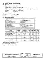
Page 17: ...cs Format Four lines of 20 characters Character Font 5x7 dot matrix with cursor Character Height w cursor 0 48 12 1mm Character Height w o cursor 0 39 9 9mm Character Width 0 24 6 1mm Overall Active Area 5 70 x 2 34 144 9mm x 59 5mm Peak Vertical Viewing Angle 20 below normal plane Viewing Mode Transflective light field Item Symbol Condition Min Typ Max Unit Viewing Angle Vertical φ1 φ2 CR 2 0 θ 0...

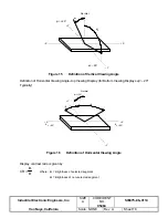
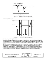
Page 18: ...Figure 15 Definition of Vertical Viewing Angle Definition of Horizontal Viewing Angle top Viewing Display for Bottom Viewing Displays φ 20 Typically X X Y Y Normal φ 20º θ θ θ 90º θ 90º Figure 16 Definition of Horizontal Viewing Angle Display contrast ratio is given by CR B B 2 1 Where B1 Brightness of selected segment B2 Brightness of non selected segment ...

Page 19: ...ard potentiometer This is considered to be a nominal adjustment but the user may prefer to vary this to optimize the viewing for a particular application The bias voltage is measured between VCC pin 22 and VBIAS pin 2 The viewing angle and contrast ratio may be externally controlled using an additional 10K ohm potentiometer The potentiometer on the rear of the module must first be set to the maxim...

Page 20: ...C Because the attenuation of the LCD cell only 10 of the backlight luminance is emitted from the display Thus to provide a brightly lit display the original light source must be 10 times brighter 7 2 Lamps Characteristics The standard light source is a 4 85 Watt 5 0 Volt halogen lamp Figure 19 below shows the standard light source and two alternates which use less power They may be satisfactory fo...

Page 21: ...w material It is also recommended that an air gap of at least 030 to 050 minimum be provided between the window material and the surface of the LCD to prevent the transfer of static charges to the front surface of the LCD Supertwist LCD s may activate un driven elements in response to a surface static charge on the front polarizer It may take several minutes for such a surface static charge to dis...

Page 22: ...dustrial Electronic Engineers Inc SIZE A CODE IDENT NO 05464 S03875 06 0114 Van Nuys California Scale NONE Rev A Sheet 22 10 0 OUTLINE AND MOUNTING CHARACTERISTICS Figure 20 03875 06 0114 Outline Drawing ...

Reviews: