WAFER-JL-N5105 SBC
Page 17
3.2.1
AT/ATX Power Mode Setting
CN Label:
J_ATX_AT1
CN Type:
3-pin switch
CN Location:
See
CN Pinouts:
See Table 3-4
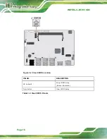
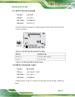
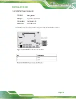
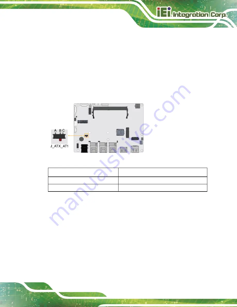
The AT/ATX power mode selection is made through the AT/ATX power mode switch which
is shown in Figure3-3.
Figure 3-3: AT/ATX Power Mode Switch Locations
PIN NO.
DESCRIPTION
Short A - B
ATX Power Mode (default)
Short B – C
AT Power Mode
Table 3-4: AT/ATX Power Mode Switch Pinouts
3.2.2
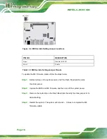
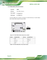
ME Override Setting Jumper
CN Label:
ME_FLASH1
CN Type:
2-pin header,P=1.27mm
CN Location:
See
CN Pinouts:
The ME_FLASH1 connector is used for Flash Descriptor Security Overide or ME Debug
Mode.
Summary of Contents for 167320
Page 12: ......
Page 13: ...WAFER JL N5105 SBC Page 1 Chapter 1 1 Introduction...
Page 20: ...WAFER JL N5105 SBC Page 8 Chapter 2 2 Unpacking...
Page 24: ...WAFER JL N5105 SBC Page 12 Chapter 3 3 Connectors...
Page 58: ...WAFER JL N5105 SBC Page 46 Chapter 4 4 Installation...
Page 71: ...WAFER JL N5105 SBC Page 59 Chapter 5 5 Software Drivers...
Page 74: ...WAFER JL N5105 SBC Page 62 Appendix A A Regulatory Compliance...
Page 76: ...WAFER JL N5105 SBC Page 64 B C Product Disposal Appendix B...
Page 78: ...WAFER JL N5105 SBC Page 66 Appendix C D Error Beep Code...


