background image


WAFER-JL-N5105 SBC 


Page 24 

3.2.8


LAN LED Connectors 

CN Label: 

JLAN_LED1, JLAN_LED2, JLAN_LED3 

CN Type: 

2-pin header, p=2.00 mm 

CN Location: 

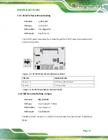
See   

Figure 3-10


CN Pinouts: 

See 

  Table 3-11, Table 3-12 

and

 Table 3-13


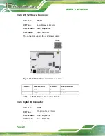
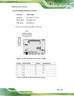
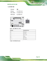
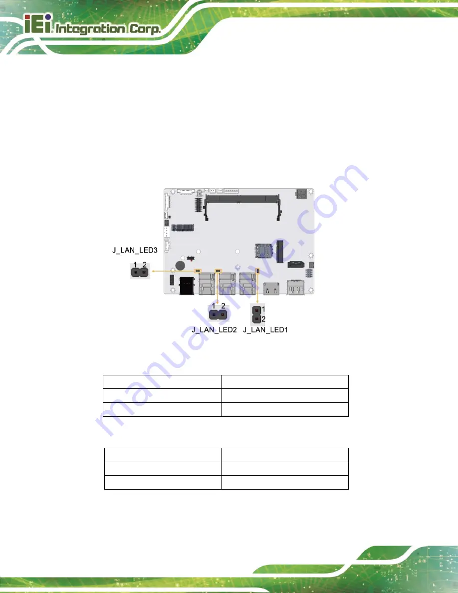
The LAN LED connectors connect to the LAN link LEDs on the system. 


Figure 3-10: LAN LED Connector Locations 


Pin 

Description 

+3.3V 

LAN1_LED_LNK#_ACT 


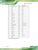
Table 3-11: LAN1 LED Connector Pinouts 


Pin 

Description 

+3.3V 

LAN2_LED_LNK#_ACT 

Table 3-12: LAN2 LED Connector Pinouts 

Summary of Contents for 167320

Page 1: ...MODEL NAME User Manual WAFER JL N5105 MODEL 3 5 SBC with Intel 10nm Jasper Lake Celeron N5105 Processor with Dual Displays DDR4 Triple Intel 2 5 GbE USB3 2 M 2 SATA COM SoC RoHS Rev 1 00 March 25 202...

Page 2: ...WAFER JL N5105 SBC Page II MODEL NAME Revision Date Version Changes March 25 2022 1 00 Initial release...

Page 3: ...ages arising out of the use or inability to use the product or documentation even if advised of the possibility of such damages This document contains proprietary information protected by copyright Al...

Page 4: ...nal injury Warnings should be taken seriously CAUTION Cautionary messages should be heeded to help reduce the chance of losing data or damaging the product NOTE These messages inform the reader of ess...

Page 5: ...RIPHERAL INTERFACE CONNECTORS 13 3 1 1 WAFER JL N5105 Layout 13 3 1 2 Peripheral Interface Connectors 13 3 1 3 External Interface Panel Connectors 15 3 2 INTERNAL PERIPHERAL CONNECTORS 15 3 2 1 Clear...

Page 6: ...Connectors 42 3 3 1 External USB 3 2 Gen 2x1 Type A 43 3 3 1 External DisplayPort Connector 44 3 3 2 External Interface Panel Connectors 45 4 INSTALLATION 46 4 1 ANTI STATIC PRECAUTIONS 47 4 2 INSTALL...

Page 7: ...WAFER JL N5105 SBC Page VII MODEL NAME B 64 C PRODUCT DISPOSAL 64 D ERROR BEEP CODE 66 D 1 PEI BEEP CODES 67 D 2 DXE BEEP CODES 67...

Page 8: ...Figure 3 10 LAN LED Connector Locations 24 Figure 3 11 Battery Connector Location 26 Figure 3 12 Power Button Connector Location 27 Figure 3 13 Reset Button Connector Location 28 Figure 3 14 RS 232 Se...

Page 9: ...Heat Sink Retention Screws 51 Figure 4 5 Active Cooling 52 Figure 4 6 Passive Cooling 52 Figure 4 7 DRPC W JL R10 52 Figure 4 8 DRPC W JL R10 with Extra Fan Cooling 52 Figure 4 9 Motherboard Installat...

Page 10: ...Connector Pinouts 23 Table 3 11 LAN1 LED Connector Pinouts 24 Table 3 12 LAN2 LED Connector Pinouts 24 Table 3 13 LAN3 LED Connector Pinouts 25 Table 3 14 Battery Connector Pinouts 26 Table 3 15 Powe...

Page 11: ...WAFER JL N5105 SBC Page XI MODEL NAME Table 3 29 External Display Port Connector Pinouts 44 Table 3 30 HDMI Connector Pinouts 45...

Page 12: ......

Page 13: ...WAFER JL N5105 SBC Page 1 Chapter 1 1 Introduction...

Page 14: ...105 series includes a HDMI1 4 up to 4096 x 2160 30Hz connector and a DP1 4 up to 4096 x 2160 60Hz connector for dual independent display Expansion and I O include one M 2 A key slot for Wi Fi or Bluet...

Page 15: ...05 on board SoC 4 cores and 4 threads 2 00GHz base frequency Three Intel I225V 2 5GbE ports Two USB 3 2 Gen 2 two USB 2 0 two RS 232 M 2 A key and M 2 B key expansions Support dual independent display...

Page 16: ...WAFER JL N5105 SBC Page 4 1 4 Dimensions The dimensions of the board are listed below Figure 1 3 Dimensions mm...

Page 17: ...WAFER JL N5105 SBC Page 5 1 5 Data Flow Shows the data flow between the system chipset the CPU and other components installed on the motherboard Figure 1 4 Data Flow Diagram...

Page 18: ...gital I O by 14 pin 2x7 header Embedded Controller ITE IT5571E Watchdog Timer Software programmable support 1 255 sec system reset I O Interface Audio Connector 1 x IAUDIO supports IEI AC KIT 888S Aud...

Page 19: ...pply 12 V DC input only AT ATX support Power Connector 1 x Internal power connector by 4 pin 2x2 connector Power Consumption 12V 2 45A Intel Pentium Silver N6000 3 30 GHz TDP 6W with one 16GB 2933MHz...

Page 20: ...WAFER JL N5105 SBC Page 8 Chapter 2 2 Unpacking...

Page 21: ...charge Self grounding Touch a grounded conductor every few minutes to discharge any excess static buildup Use an anti static pad When configuring any circuit board place it on an anti static mat Only...

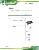
Page 22: ...seller or vendor the WAFER JL N5105 was purchased from or contact an IEI sales representative directly by sending an email to sales ieiworld com The WAFER JL N5105 is shipped with the following compon...

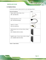
Page 23: ...Image Dual port USB 2 0 cable 210mm P 2 0 P N CB USB02A RS RS 232 cable 250 mm p 1 25 P N 32005 003500 200 RS Audio kit 7 1 Channel P N AC KIT 888S R10 Cooler module 157 mm x 100 mm x 20 mm with pad a...

Page 24: ...WAFER JL N5105 SBC Page 12 Chapter 3 3 Connectors...

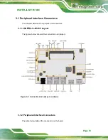
Page 25: ...is chapter details all the jumpers and connectors 3 1 1 WAFER JL N5105 Layout The figures below show all the connectors and jumpers Figure 3 1 Connector And Jumper Locations 3 1 2 Peripheral Interface...

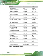
Page 26: ...onnector 2 pin header JLAN_LED2 LAN3 link LED connector 2 pin header JLAN_LED3 Battery connector 2 pin wafer BAT2 Power button connector 2 pin wafer PWR_BTN1 Reset button connector 2 pin wafer RST_BTN...

Page 27: ...al HDMI connector HDMI HDMI1 Table 3 2 Rear Panel Connectors 3 2 Internal Peripheral Connectors The section describes all of the connectors on the WAFER JL N5105 3 2 1 Clear CMOS Button CN Label J_CMO...

Page 28: ...WAFER JL N5105 SBC Page 16 Figure 3 2 Clear CMOS Location Table 3 3 Clear CMOS Pinouts PIN NO DESCRIPTION NC default Keep CMOS Setup Normal Operation Press button Clear CMOS Setup...

Page 29: ...switch which is shown in Figure3 3 Figure 3 3 AT ATX Power Mode Switch Locations PIN NO DESCRIPTION Short A B ATX Power Mode default Short B C AT Power Mode Table 3 4 AT ATX Power Mode Switch Pinouts...

Page 30: ...g on the system power short the Flash Descriptor Security Override jumper Step 2 Update the BIOS and ME firmware and then turn off the system power Step 3 Remove the metal clip on the Flash Descriptor...

Page 31: ...connected to external audio devices AC KIT 888S R10 including speakers and microphones for the input and output of audio signals to and from the system Figure 3 5 Audio Connector Location Table 3 6 A...

Page 32: ...uts See Table 3 7 The connector supports the 12V power supply Figure 3 6 ATX 12V Power Connector Location PIN NO DESCRIPTION PIN NO DESCRIPTION 1 GND 2 GND 3 12V 4 12V Table 3 7 ATX 12V Power Connecto...

Page 33: ...rammable input and output for external devices Figure 3 7 Digital I O Connector Location PIN NO DESCRIPTION PIN NO DESCRIPTION 1 GND 2 VCC 3 DOUT5 4 DOUT4 5 DOUT3 6 DOUT2 7 DOUT1 8 DOUT0 9 DIN5 10 DIN...

Page 34: ...FAN1 CN Type 4 pin wafer p 2 54 mm CN Location See Figure 3 8 CN Pinouts See Table 3 9 The fan connector attaches to a smart cooling fan Figure 3 8 Fan Connector Location Table 3 9 Fan Connector Pinou...

Page 35: ...Figure 3 9 CN Pinouts See Table 3 10 The front panel connector connects to the power LED indicator and HDD LED indicator on the system front panel Figure 3 9 Power LED HDD LED Connector Location Pin D...

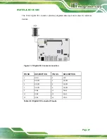
Page 36: ...ee Figure 3 10 CN Pinouts See Table 3 11 Table 3 12 and Table 3 13 The LAN LED connectors connect to the LAN link LEDs on the system Figure 3 10 LAN LED Connector Locations Pin Description 1 3 3V 2 LA...

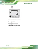
Page 37: ...board battery Dispose of used batteries according to instructions and local regulations NOTE It is recommended to attach the RTC battery onto the system chassis in which the WAFER JL N5105 is install...

Page 38: ...WAFER JL N5105 SBC Page 26 Figure 3 11 Battery Connector Location Pin Description 1 VBAT 2 GND Table 3 14 Battery Connector Pinouts...

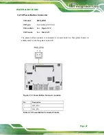
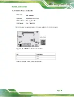
Page 39: ...m CN Location See Figure 3 12 CN Pinouts See Table 3 15 The power button connector is connected to a power switch on the system chassis to enable users to turn the system on and off Figure 3 12 Power...

Page 40: ...ation See Figure 3 13 CN Pinouts See Table 3 16 The reset button connector is connected to a reset switch on the system chassis to enable users to reboot the system when the system is turned on Figure...

Page 41: ...p 1 25 mm CN Location See Figure 3 14 CN Pinouts See Table 3 17 The serial connector provides RS 232 connection Figure 3 14 RS 232 Serial Port Connector Location PIN NO DESCRIPTION PIN NO DESCRIPTION...

Page 42: ...See Table 3 18 The SATA 6Gb s drive connector is connected to a SATA 6Gb s drive The SATA 6Gb s drive transfers data at speeds as high as 6Gb s Figure 3 15 SATA 6Gb s Drive Connectors Location PIN NO...

Page 43: ...WR1 CN Type 2 pin wafer p 2 00 mm CN Location See Figure 3 16 CN Pinouts See Table 3 19 The SATA power connector provides 5 V power output to the SATA connector Figure 3 16 SATA Power Connector Locati...

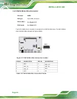
Page 44: ...afer p 1 25 mm CN Location See Figure 3 17 CN Pinouts See Table 3 20 The SMBus System Management Bus connector provides low speed system management communications Figure 3 17 SMBus Connector Location...

Page 45: ...6 pin wafer p 1 25 mm CN Location See Figure 3 18 CN Pinouts See Table 3 21 The 6 pin SPI Flash connector is used to flash the BIOS Figure 3 18 SPI Flash Connector Location Pin Description 1 3 3V 2 SP...

Page 46: ...CN Location See Figure 3 19 CN Pinouts See Table 3 22 The USB connector provides two USB 2 0 ports by dual port USB cable Figure 3 19 USB Connector Location PIN NO DESCRIPTION PIN NO DESCRIPTION 1 VC...

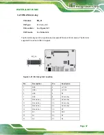
Page 47: ...and USB 2 0 signal supports NVMe storage or 5G module with SIM holder Figure 3 20 M 2 B key Slot Location PIN NO DESCRIPTION PIN NO DESCRIPTION 1 CONFIG_3 2 3 3V 3 GND 4 3 3V 5 GND 6 POWER_OFF 7 USB_D...

Page 48: ...TXP1 38 DEVSLP 39 GND 40 N C 41 PCIE_RXN0 42 N C 43 PCIE_RXP0 44 N C 45 GND 46 N C 47 PCIE_TXN0 48 N C 49 PCIE_TXP0 50 PERST 51 GND 52 CLKREQ 53 REFCLKN 54 PEWAKE 55 REFCLKP 56 N C 57 GND 58 N C 59 N...

Page 49: ...he A position and accepts 2230 size of M 2 modules The M 2 slot supports PCIe x2 and USB 2 0 signals Figure 3 21 M 2 A key Slot Location Pin Description Pin Description 1 GND 2 V3 3A 3 USB 4 V3 3A 5 U...

Page 50: ...GND 40 NC 41 PCIE_RX0 42 NC 43 PCIE_RX0 44 NC 45 GND 46 NC 47 CLK_PCIE0 48 NC 49 CLK_PCIE0 50 NC 51 GND 52 BUF_PLT_RST 53 PCIE_CLKREQ 54 Pull Up V3 3A 55 PCIE_WAKE 56 Pull Up V3 3A 57 GND 58 NC 59 PCI...

Page 51: ...lot CN Label SIM1 CN Type 7 PIN SIM holder CN Location See Figure 3 22 CN Pinouts See Table 3 25 Figure 3 22 SIM Slot Location PIN NO DESCRIPTION C1 SIM_VCC C2 SIM_RST C3 SIM_Clock C5 GND C6 SIM_VPP C...

Page 52: ...BC Page 40 3 2 21 DDR4 SO DIMM Socket CN Label DIMM_A1 CN Type 260 pin DDR4 SO DIMM socket CN Location See 791HFigure 3 23 The SO DIMM slot is for installing the DDR4 SO DIMM Figure 3 23 DDR4 SO DIMM...

Page 53: ...tor Panel Figure 3 24 shows the WAFER JL N5105 external peripheral interface connector EPIC panel The EPIC panel consists of the following 1x HDMI 1 x DP connector 3 x GbE RJ 45 connector 2x USB 3 2 G...

Page 54: ...8HFigure 3 25 CN Pinouts See 809HTable 3 26 The LAN connector connects to a local network LAN LED location and pinouts see Figure 3 26 and Table 3 27 Figure 3 25 LAN Location Pin Description Pin Descr...

Page 55: ...outs 3 3 1 External USB 3 2 Gen 2x1 Type A CN Label USB1 USB2 CN Type USB 3 2 Gen 2 port Type A CN Location See 814HFigure 3 27 CN Pinouts See 815H Table 3 28 The WAFER JL N5105 has four external USB...

Page 56: ...Table 3 28 USB 3 2 Gen 2 Port Pinouts 3 3 1 External DisplayPort Connector CN Label DP1 CN Type External DP connector CN Location See Figure 3 28 CN Pinouts See Table 3 29 PIN NO DESCRIPTION PIN NO DE...

Page 57: ...CN Pinouts See Table 3 30 The HDMI connectors can connect to HDMI devices Pin Description Pin Description 1 HDMI2_DATA2 2 GND 3 HDMI2_DATA2 4 HDMI2_DATA1 5 GND 6 HDMI2_DATA1 7 HDMI2_DATA0 8 GND 9 HDM...

Page 58: ...WAFER JL N5105 SBC Page 46 Chapter 4 4 Installation...

Page 59: ...tband can help to prevent ESD from damaging the board Self grounding Before handling the board touch any grounded conducting material During the time the board is handled frequently touch any conducti...

Page 60: ...D from the body and helps prevent ESD damage Place the WAFER JL N5105 on an antistatic pad o When installing or configuring the motherboard place it on an antistatic pad This helps to prevent potentia...

Page 61: ...ep 2 Align the SO DIMM with the socket Align the notch on the memory with the notch on the memory socket Step 3 Insert the SO DIMM Push the memory in at a 20 angle See Figure 4 1 Step 4 Seat the SO DI...

Page 62: ...ve the retention screw secured on the motherboard Step 3 Line up the notch on the module with the notch on the slot Slide the M 2 module into the socket at an angle of about 20 Figure 4 2 Figure 4 2 I...

Page 63: ...r directly on a surface that cannot dissipate system heat and never run the WAFER JL N5105 without the heat spreader secured to the board When the WAFER JL N5105 is shipped it is secured to a heat spr...

Page 64: ...P N 19XM0B619 0002002 000 RS see Figure 4 6 Figure 4 5 Active Cooling Figure 4 6 Passive Cooling 4 5 1 Motherboard Installation IEI recommend you to choose the DRPC W JL for the WAFER JL N5105 install...

Page 65: ...n the heat spreader for installing the WAFER JL N5105 The following diagram shows an example of motherboard installation Figure 4 9 Motherboard Installation Example 4 6 Internal Peripheral Device Conn...

Page 66: ...in 2x2 Molex type power cable connector to the power connector on the motherboard See Figure 4 10 Figure 4 10 Power Cable to Motherboard Connection Step 3 Connect power cable to power supply Connect o...

Page 67: ...eller or vendor or contact an IEI sales representative directly The audio kit attaches to the audio connector The audio kit provides 7 1 channel audio To install the audio kit please refer to the step...

Page 68: ...urces to the audio jacks on the audio kit Step 5 Install the driver Install the 7 1 channel audio driver included with the board Step 0 4 6 3 RS 232 Cable Connection The single RS 232 cable consists o...

Page 69: ...r bracket Step 4 Connect the serial device Once the single RS 232 connector is connected to a chassis or bracket a serial communications device can be connected to the system Step 0 4 6 4 SATA Drive C...

Page 70: ...ion Step 3 Connect the cable to the SATA disk Connect the connector on the other end of the cable to the connector at the back of the SATA drive Step 4 To remove the SATA cable from the SATA connector...

Page 71: ...WAFER JL N5105 SBC Page 59 Chapter 5 5 Software Drivers...

Page 72: ...to find all the relevant software utilities and documentation Figure 5 1 IEI Resource Download Center 5 2 Driver Download To download drivers from IEI Resource Download Center follow the steps below S...

Page 73: ...e following window You can download the entire ISO file or click the small arrow to find an individual driver and click the file name to download NOTE To install software from the downloaded ISO image...

Page 74: ...WAFER JL N5105 SBC Page 62 Appendix A A Regulatory Compliance...

Page 75: ...rence that may cause undesired operation This equipment has been tested and found to comply with the limits for a Class A digital device pursuant to part 15 of the FCC Rules These limits are designed...

Page 76: ...WAFER JL N5105 SBC Page 64 B C Product Disposal Appendix B...

Page 77: ...fied as electronic device in terms of the European Directive 2012 19 EU WEEE and must not be disposed of as domestic garbage EU wide legislation as implemented in each Member State requires that waste...

Page 78: ...WAFER JL N5105 SBC Page 66 Appendix C D Error Beep Code...

Page 79: ...found 4 Recovery failed 4 S3 Resume failed 7 Reset PPI is not available D 2 DXE Beep Codes Number of Beeps Description 1 Invalid password 4 Some of the Architectural Protocols are not available 5 No...

Reviews: