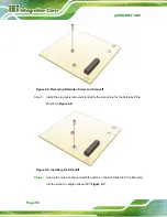
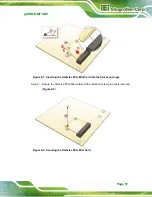
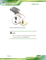
background image


gKINO-DMF SBC

Page 58 

4.6 System Configuration 

The system configuration is controlled by buttons, jumpers and switches. The system 

configuration should be performed before installation. 

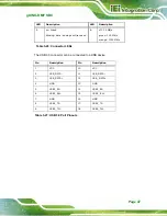
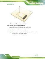
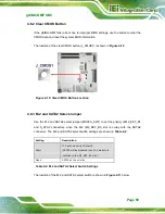
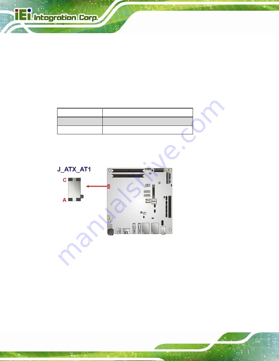
4.6.1 AT/ATX Mode Select Switch 

The AT/ATX mode select switch (J_ATX_AT1) specifies the systems power mode as AT 

or ATX. AT/ATX mode select switch settings are shown in 

Table 4-1

Setting Description 

Short A-B 

ATX Mode (Default) 

Short B-C 

AT Mode  

Table 4-1: AT/ATX Mode Select Switch Settings 

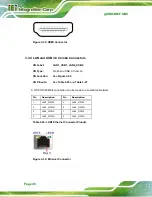
The location of the AT/ATX mode select switch is shown in 

Figure 4-9 

below. 


Figure 4-9: AT/ATX Mode Select Switch Location 

Summary of Contents for gKINO-DMF-216-R10

Page 1: ...r Manual gKINO DMF MODEL Mini ITX SBC with AMD Embedded R Series On board SoC DisplayPort Dual PCIe GbE USB 3 0 PCIe Mini M 2 PCIe x8 SATA 6Gb s RS 232 422 485 ccTalk Audio TPM and RoHS Rev 1 00 June 29 2017 gKINO DMF CPU Card ...

Page 2: ...gKINO DMF SBC Page II Revision Date Version Changes June 29 2017 1 00 Initial release ...

Page 3: ...ising out of the use or inability to use the product or documentation even if advised of the possibility of such damages This document contains proprietary information protected by copyright All rights are reserved No part of this manual may be reproduced by any mechanical electronic or other means in any form without prior written permission of the manufacturer TRADEMARKS All registered trademark...

Page 4: ...autionary messages should be heeded to help reduce the chance of losing data or damaging the product NOTE These messages inform the reader of essential but non critical information These messages should be read carefully as any directions or instructions contained therein can help avoid making mistakes HOT SURFACE This symbol indicates a hot surface that should not be touched without taking care ...

Page 5: ...ITEMS 14 3 CONNECTORS 15 3 1 PERIPHERAL INTERFACE CONNECTORS 16 3 1 1 gKINO DMF Layout 16 3 1 2 Peripheral Interface Connectors 18 3 1 3 External Interface Panel Connectors 19 3 2 INTERNAL PERIPHERAL CONNECTORS 20 3 2 1 12 V DC IN Power Connector 20 3 2 2 Audio Connector 21 3 2 3 Battery Connector 22 3 2 4 ccTalk Connectors 23 3 2 5 Chassis Intrusion Connector 24 3 2 6 Digital I O Connector 25 3 2...

Page 6: ...ERAL INTERFACE CONNECTOR PANEL 43 3 3 1 Audio Jacks 43 3 3 2 DisplayPort Connector 44 3 3 3 HDMI Connectors 45 3 3 4 LAN and USB 3 0 Combo Connectors 46 3 3 5 Power Connector 48 3 3 6 USB 2 0 Connector 48 4 INSTALLATION 49 4 1 ANTI STATIC PRECAUTIONS 50 4 2 INSTALLATION CONSIDERATIONS 50 4 3 SO DIMM INSTALLATION 52 4 4 M 2 MODULE INSTALLATION 53 4 5 PCIE MINI CARD INSTALLATION 53 4 5 1 Full size P...

Page 7: ...erial Port n Configuration 71 5 3 4 1 1 Serial Port 1 Configuration 72 5 3 4 1 2 Serial Port 2 Configuration 73 5 3 4 1 3 Serial Port 3 Configuration 74 5 3 4 1 4 Serial Port 4 Configuration 75 5 3 4 1 5 Serial Port 5 Configuration 76 5 3 4 1 6 Serial Port 6 Configuration 77 5 3 5 iWDD H W Monitor 79 5 3 5 1 Smart Fan Mode Configuration 80 5 3 6 RTC Wake Settings 82 5 3 7 Power Saving Configuratio...

Page 8: ... SAVE EXIT 96 6 SOFTWARE DRIVERS 98 6 1 SOFTWARE INSTALLATION 99 6 2 AVAILABLE SOFTWARE DRIVERS 100 A REGULATORY COMPLIANCE 101 B PRODUCT DISPOSAL 103 C BIOS MENU OPTIONS 105 D TERMINOLOGY 108 E DIGITAL I O INTERFACE 112 F WATCHDOG TIMER 115 G HAZARDOUS MATERIALS DISCLOSURE 118 ...

Page 9: ... Connector Locations 26 Figure 3 9 Front Panel Connector Location 27 Figure 3 10 I2 C Connector Location 28 Figure 3 11 LAN LED Connector Locations 29 Figure 3 12 M 2 Slot Location 30 Figure 3 13 microSD Card Slot Location 31 Figure 3 14 PCIe Mini Card Slot Location 32 Figure 3 15 PCIe x1 Slot Location 33 Figure 3 16 RS 232 Serial Port Connector Locations 34 Figure 3 17 RS 232 422 485 Connector Lo...

Page 10: ... at an Angle 54 Figure 4 4 Securing the Full size PCIe Mini Card 55 Figure 4 5 Removing Retention Screw and Standoff 56 Figure 4 6 Installing the Standoff 56 Figure 4 7 Inserting the Half size PCIe Mini Card into the Slot at an Angle 57 Figure 4 8 Securing the Half size PCIe Mini Card 57 Figure 4 9 AT ATX Mode Select Switch Location 58 Figure 4 10 Clear CMOS Button Location 59 Figure 4 11 M 2 and ...

Page 11: ...ctor Pinouts 28 Table 3 12 LAN LED Connector Pinouts 29 Table 3 13 PCIe Mini Card Slot Pinouts 33 Table 3 14 RS 232 Serial Port Connector Pinouts 34 Table 3 15 RS 232 422 485 Connector Pinouts 35 Table 3 16 DB 9 RS 422 485 Pinouts 36 Table 3 17 SATA Power Connector Pinouts 37 Table 3 18 SMBus Connector Pinouts 38 Table 3 19 SPI Flash Connector Pinouts 39 Table 3 20 SPI Flash Connector Pinouts 40 T...

Page 12: ...gKINO DMF SBC Page XII Table 4 2 M 2 and SATA2 Select Switch Settings 59 Table 5 1 BIOS Navigation Keys 65 ...

Page 13: ...onitor 79 BIOS Menu 9 Smart Fan Mode Configuration 80 BIOS Menu 10 RTC Wake Settings 82 BIOS Menu 11 Power Saving Configuration 83 BIOS Menu 12 CPU Configuration 85 BIOS Menu 13 Node 0 Information 86 BIOS Menu 14 NVMe Configuration 86 BIOS Menu 15 USB Configuration 87 BIOS Menu 16 Chipset 88 BIOS Menu 17 South Bridge 89 BIOS Menu 18 SB SATA Configuration 90 BIOS Menu 19 GFX Configuration 91 BIOS M...

Page 14: ......

Page 15: ...gKINO DMF SBC Page 1 Chapter 1 1 Introduction ...

Page 16: ...rs and one external Dual mode DisplayPort DisplayPort connector for triple independent display which support up to 4K resolution Expansion and I O include one PCIe x8 slot one PCIe Mini slot one M 2 B key slot for expansion four USB 3 0 connectors on the rear panel four USB 2 0 connectors by pin header and two SATA 6Gb s connectors Serial device connectivity is provided by two internal RS 232 conn...

Page 17: ...atures are listed below Mini ITX motherboard supports AMD RX 421BD or RX 216GD on board SoC Triple independent display via HDMI 1 4 and DP Two 2400 MHz DDR4 SO DIMM slots support up to 64 GB of memory Two SATA 6Gb s connectors with 5 V power output Full size half size PCIe Mini card slot for expansion M 2 B key modules supported Support microSD card for data storage One PCIe x8 slot for expansions...

Page 18: ...gKINO DMF SBC Page 4 1 4 Connectors The connectors on the gKINO DMF are shown in the figures below Figure 1 2 Connectors Front Side ...

Page 19: ...gKINO DMF SBC Page 5 Figure 1 3 Connectors Solder Side ...

Page 20: ...gKINO DMF SBC Page 6 1 5 Dimensions The dimensions of the board are listed below Figure 1 4 Dimensions mm ...

Page 21: ...gKINO DMF SBC Page 7 1 6 Data Flow Figure 1 5 shows the data flow between the system chipset the CPU and other components installed on the motherboard Figure 1 5 Data Flow Diagram ...

Page 22: ...0000 graphics 3rd Gen graphics core supporting DX 12 HSA 2 0 UVD v6 decode for H 265 MPEG2 4 VC 1 MVC VCE v3 1 encode for H 254 VCE Display Output Triple independent display 2 x HDMI 1 4 up to 4096x2160 24Hz 1 x DisplayPort up to 3840x2160 60Hz Ethernet Dual Realtek RTL8119I PCIe GbE controller Digital I O 8 bit digital I O by 10 pin 2x5 header Super IO Fintek F81866 Audio Realtek ALC662 HD audio ...

Page 23: ...4 pin 1x4 wafer SMBus 1 x SMBus connector by 4 pin 1x4 wafer I2 C 1 x I2 C connector by 4 pin 1x4 wafer TPM 1 x TPM connector by 20 pin 2x10 header Chassis Intrusion Detection 1 x Chassis intrusion connector by 2 pin 1x2 header Storage 2 x SATA 6Gb s with 5 V SATA power connectors 1 x M 2 slot B key SATA 2 port USB 2 0 signal 1 x microSD socket Expansion 1 x Full size Half size PCIe Mini card slot...

Page 24: ...MF SBC Page 10 Specification gKINO DMF Storage Temperature 10 C 70 C Humidity 5 95 non condensing Physical Specifications Dimensions 170 mm x 170 mm Weight GW NW 1100 g 700 g Table 1 2 Technical Specifications ...

Page 25: ...gKINO DMF SBC Page 11 Chapter 2 2 Unpacking ...

Page 26: ...scharge Self grounding Touch a grounded conductor every few minutes to discharge any excess static buildup Use an anti static pad When configuring any circuit board place it on an anti static mat Only handle the edges of the PCB Don t touch the surface of the motherboard Hold the motherboard by the edges when handling 2 2 Unpacking Precautions When the gKINO DMF is unpacked please do the following...

Page 27: ...n Contact the IEI reseller or vendor the gKINO DMF was purchased from or contact an IEI sales representative directly by sending an email to sales ieiworld com The gKINO DMF is shipped with the following components Quantity Item and Part Number Image 1 gKINO DMF single board computer 1 SATA cable 1 I O shielding 1 Utility CD 1 One Key Recovery CD ...

Page 28: ...ms The following are optional components which may be separately purchased Item and Part Number Image Dual USB cable with bracket 300mm P 2 0 P N CB USB02A RS RS 232 cable 300mm P 2 0 P N 19800 000300 100 RS Infineon TPM module 20 pin firmware v3 17 P N TPM IN01 R20 ...

Page 29: ...gKINO DMF SBC Page 15 Chapter 3 3 Connectors ...

Page 30: ...ge 16 3 1 Peripheral Interface Connectors This chapter details all the jumpers and connectors 3 1 1 gKINO DMF Layout The figures below show all the connectors and jumpers Figure 3 1 Connector and Jumper Locations Front ...

Page 31: ...gKINO DMF SBC Page 17 Figure 3 2 Connector and Jumper Locations Rear ...

Page 32: ...header DIO1 Fan connector CPU 4 pin wafer CPU_FAN1 Fan connector system 4 pin wafer SYS_FAN1 Front panel connector 10 pin header F_PANEL1 I2 C connector 4 pin wafer I2C1 LAN LED connectors 2 pin header LED_LAN1 LED_LAN2 M 2 slot M 2 B key slot M2_KEY_B1 Memory slot 260 pin DDR4 SO DIMM DIMMA_1 DIMMB_1 microSD slot solder side microSD slot SD1 PCIe Mini card slot PCIe Mini slot MPCIE1 PCIe x8 slot ...

Page 33: ... TPM1 USB 2 0 connector 8 pin header USB1 USB2 Table 3 1 Peripheral Interface Connectors 3 1 3 External Interface Panel Connectors The table below lists the connectors on the external I O panel Connector Type Label 12 V DC IN power jack Power jack PWR_IN1 Audio jacks Audio jack AUDIO_CV1 DisplayPort connector DisplayPort DP1 HDMI connectors HDMI HDMI_CN1 HDMI_CN2 LAN and USB 3 0 combo connectors R...

Page 34: ...MF 3 2 1 12 V DC IN Power Connector CN Label CPU12V1 CN Type 4 pin Molex p 4 2 mm CN Location See Figure 3 3 CN Pinouts See Table 3 3 The connector supports the 12 V power supply Figure 3 3 DC IN Power Connector Location Pin Description Pin Description 1 GND 2 GND 3 12V 4 12V Table 3 3 DC IN Power Connector Pinouts ...

Page 35: ...supporting High Definition Audio is connected to external audio devices including speakers and microphones for the input and output of audio signals to and from the system Figure 3 4 Audio Connector Location Pin Description Pin Description 1 LMIC2 L 2 GND 3 LMIC2 R 4 Pre Sense 5 LLINE2 R 6 MIC2 JD 7 FRONT IO 8 NC 9 LLINE2 L 10 LINE2 JD Table 3 4 Audio Connector Pinouts ...

Page 36: ...cording to instructions and local regulations CN Label BAT1 CN Type 2 pin wafer p 1 25 mm CN Location See Figure 3 5 CN Pinouts See Table 3 5 The battery connector is connected to the system battery The battery provides power to the system clock to retain the time when power is turned off Figure 3 5 Battery Connector Location Pin Description 1 RTC Battery 2 RTC Battery Table 3 5 Battery Connector ...

Page 37: ...N Label J2 J3 CN Type 4 pin wafer p 2 5 mm CN Location See Figure 3 6 CN Pinouts See Table 3 6 The connectors provide ccTalk connections Figure 3 6 ccTalk Connector Locations Pin Description 1 12V 2 NC 3 GND 4 DATA Table 3 6 ccTalk Connector Pinouts ...

Page 38: ...See Figure 3 7 CN Pinouts See Table 3 7 The chassis intrusion connector is for a chassis intrusion detection sensor or switch that detects if a chassis component is removed or replaced Figure 3 7 Chassis Intrusion Connector Location Pin Description 1 V3 3VSB 2 CHASSIS OPEN Table 3 7 Chassis Intrusion Connector Pinouts ...

Page 39: ...N Pinouts See Table 3 8 The 8 bit digital I O connector provides programmable input and output for external devices Figure 3 8 Digital I O Connector Location Pin Description Pin Description 1 GND 2 VCC 3 Output 3 4 Output 2 5 Output 1 6 Output 0 7 Input 3 8 Input 2 9 Input 1 10 Input 0 Table 3 8 Digital I O Connector Pinouts ...

Page 40: ...CPU_FAN1 SYS_FAN1 CN Type 4 pin wafer p 2 54 mm CN Location See Figure 3 9 CN Pinouts See Table 3 9 The fan connector attaches to a cooling fan Figure 3 9 Fan Connector Locations Pin Description 1 GND 2 12V 3 FAN_IO 4 PWM Table 3 9 Fan Connector Pinouts ...

Page 41: ... CN Pinouts See Table 3 10 The front panel connector connects to the indicator LEDs and buttons on the system front panel Figure 3 10 Front Panel Connector Location Pin Description Pin Description 1 NC 6 PWR_LED 2 PWR_BTN 7 PWR_LED 3 PWR_BTN 8 PWR_LED 4 HDD_LED 9 RESET 5 HDD_LED 10 RESET Table 3 10 Front Panel Connector Pinouts ...

Page 42: ... 4 pin wafer p 1 25 mm CN Location See Figure 3 11 CN Pinouts See Table 3 11 The I2 C connector is used to connect I2 C bus devices to the mainboard Figure 3 11 I2 C Connector Location Pin Description 1 GND 2 I2C_DAT 3 I2C_CLK 4 5V Table 3 11 I2 C Connector Pinouts ...

Page 43: ...AN2 CN Type 2 pin header p 2 54 mm CN Location See Figure 3 12 CN Pinouts See Table 3 12 The LAN LED connectors connect to the LAN link LEDs on the system Figure 3 12 LAN LED Connector Locations Pin Description 1 3 3V 2 LAN_LED_LNK _ACT Table 3 12 LAN LED Connector Pinouts ...

Page 44: ...r the SATA2 connector or the M 2 module for storage CN Label M2_KEY_B1 CN Type M 2 B key slot CN Location See Figure 3 13 The M 2 slot is keyed in the B position The M 2 slot supports SATA and USB 2 0 interfaces only The optional M 2 module especially designed for the gKINO DMF can be installed into this M 2 slot vertically Figure 3 13 M 2 Slot Location ...

Page 45: ... on the solder side accepts a microSD card for storage Figure 3 14 microSD Card Slot Location 3 2 13 PCIe Mini Card Slot CN Label MPCIE1 CN Type Half size Full size PCIe Mini card slot CN Location See 5Figure 3 15 CN Pinouts See Table 3 13 The PCIe Mini card slot is for installing a full size or half size PCIe Mini expansion card ...

Page 46: ...5 N C 6 1 5V 7 N C 8 N C 9 GND 10 N C 11 MSATA_CLK 12 N C 13 MSATA _CLK 14 N C 15 GND 16 N C 17 PLTRST_N 18 GND 19 N C 20 3 3V 21 GND 22 PLTRST_N 23 MINI_RXN 24 3 3V 25 MINI_RXP 26 GND 27 GND 28 1 5V 29 GND 30 SMB_CLK 31 MINI_TXN 32 SMB_DATA 33 MINI_TXP 34 GND 35 GND 36 USB_DATA 37 GND 38 USB_DATA 39 3 3V 40 GND 41 3 3V 42 N C ...

Page 47: ...K 46 N C 47 CLINK_DATA 48 1 5V 49 CLINK_RST 50 GND 51 MSATA_DET 52 3 3V Table 3 13 PCIe Mini Card Slot Pinouts 3 2 14 PCIe x8 Card Slot CN Label PCIE1 CN Type PCIe x8 slot CN Location See 5Figure 3 16 The PCIe x8 slot is for PCIe x8 expansion cards Figure 3 16 PCIe x1 Slot Location ...

Page 48: ...p 2 00 mm CN Location See Figure 3 17 CN Pinouts See Table 3 14 The serial connectors provide RS 232 connections Figure 3 17 RS 232 Serial Port Connector Locations Pin Description Pin Description 1 DCD 2 DSR 3 RX 4 RTS 5 TX 6 CTS 7 DTR 8 RI 9 GND 10 GND Table 3 14 RS 232 Serial Port Connector Pinouts ...

Page 49: ...e default mode is set to RS 232 To configure the connectors as RS 422 or RS 485 please refer to Section 5 3 4 1 5 and Section 5 3 4 1 6 Figure 3 18 RS 232 422 485 Connector Locations PIN NO DESCRIPTION PIN NO DESCRIPTION 1 DCD 2 DSR 3 RXD 4 RTS 5 TXD 6 CTS 7 DTR 8 RI 9 GND 10 GND Table 3 15 RS 232 422 485 Connector Pinouts Use the optional RS 232 422 485 cable to connect to a serial device The pin...

Page 50: ...outs 3 2 17 SATA 6Gb s Drive Connectors CN Label S_ATA1 S_ATA2 CN Type 7 pin SATA connector CN Location See Figure 3 19 The SATA 6Gb s drive connector is connected to a SATA 6Gb s drive The SATA 6Gb s drive transfers data at speeds as high as 6Gb s Figure 3 19 SATA 6Gb s Drive Connectors Locations ...

Page 51: ...TA_PWR2 CN Type 2 pin wafer p 2 00 mm CN Location See Figure 3 20 CN Pinouts See Table 3 17 The SATA power connector provides 5 V power output to the SATA connector Figure 3 20 SATA Power Connector Locations Pin Description 1 5V 2 GND Table 3 17 SATA Power Connector Pinouts ...

Page 52: ...r p 1 25 mm CN Location See Figure 3 21 CN Pinouts See Table 3 18 The SMBus System Management Bus connector provides low speed system management communications Figure 3 21 SMBus Connector Location Pin Description 1 GND 2 SMB_DATA 3 SMB_CLK 4 5V Table 3 18 SMBus Connector Pinouts ...

Page 53: ...ype 6 pin wafer p 1 25 mm CN Location See Figure 3 22 CN Pinouts See Table 3 19 The 6 pin SPI Flash connector is used to flash the BIOS Figure 3 22 SPI Flash Connector Location Pin Description 1 1 8V 2 SPI_CS 3 SPI_SO 4 SPI_CLK 5 SPI_SI 6 GND Table 3 19 SPI Flash Connector Pinouts ...

Page 54: ... 6 pin wafer p 1 25 mm CN Location See Figure 3 23 CN Pinouts See Table 3 20 The 6 pin SPI Flash connector is used to flash the EC Figure 3 23 SPI Flash Connector Location Pin Description 1 1 8V 2 SPI_CS 3 SPI_SO 4 SPI_CLK 5 SPI_SI 6 GND Table 3 20 SPI Flash Connector Pinouts ...

Page 55: ...Table 3 21 The Trusted Platform Module TPM connector secures the system on bootup Figure 3 24 TPM Connector Location Pin Description Pin Description 1 LCLK 2 GND 3 LFRAME 4 KEY 5 LRERST 6 5V 7 LAD3 8 LAD2 9 3 3V 10 LAD1 11 LAD0 12 GND 13 SCL 14 SDA 15 SB3V 16 SERIRQ 17 GND 18 CLKRUN 19 LPCPD 20 LDRQ Table 3 21 TPM Connector Pinouts ...

Page 56: ...der p 2 0 mm CN Location See Figure 3 25 CN Pinouts See Table 3 22 The USB connectors provide four USB 2 0 ports by dual port USB cable Figure 3 25 USB Connector Locations Pin Description Pin Description 1 5V 2 GND 3 DATA 4 DATA 5 DATA 6 DATA 7 GND 8 5V Table 3 22 USB Connector Pinouts ...

Page 57: ...ower jack PWR_IN1 1 x DisplayPort connector DP1 2 x GbE and USB 3 0 combo connector LAN1_USB1 LAN2_USB2 2 x HDMI connector HDMI_CN1 HDMI_CN2 1 x USB 2 0 connector EXT_USB2 Figure 3 26 External Peripheral Interface Connector 3 3 1 Audio Jacks CN Label AUDIO_CV1 CN Type Audio jack CN Location See Figure 3 26 The audio jacks connect to external audio devices Line In port Light Blue Connects a CD ROM ...

Page 58: ...ector CN Label DP1 CN Type DisplayPort connector CN Location See Figure 3 26 CN Pinouts See Table 3 23 The DisplayPort connector can connect to a DisplayPort device or the user can use a passive adapter to convert DisplayPort signals to single link HDMI or DVI Pin Description Pin Description 1 5V 11 AUXP 2 LANE1N 12 AUXN 3 LANE1P 13 GND 4 GND 14 LANE2P 5 LANE3N 15 LANE2N 6 LANE3P 16 GND 7 GND 17 L...

Page 59: ... HDMI port CN Location See Figure 3 26 CN Pinouts See Table 3 24 The HDMI connector can connect to an HDMI device Pin Description Pin Description 1 HDMI_DATA2 13 N C 2 GND 14 N C 3 HDMI_DATA2 15 HDMI_SCL 4 HDMI_DATA1 16 HDMI_SDA 5 GND 17 GND 6 HDMI_DATA1 18 5V 7 HDMI_DATA0 19 HDMI_HPD 8 GND 20 HDMI_GND 9 HDMI_DATA0 21 HDMI_GND 10 HDMI_CLK 22 HDMI_GND 11 GND 23 HDMI_GND 12 HDMI_CLK Table 3 24 HDMI ...

Page 60: ...o CN Location See 5Figure 3 26 CN Pinouts See 5Table 3 25 and Table 3 27 A 10 100 1000 Mb s connection can be made to a Local Area Network Pin Description Pin Description 1 LAN1_MDI0P 5 LAN1_MDI2P 2 LAN1_MDI0N 6 LAN1_MDI2N 3 LAN1_MDI1P 7 LAN1_MDI3P 4 LAN1_MDI1N 8 LAN1_MDI3N Table 3 25 LAN1 Ethernet Connector Pinouts Figure 3 30 Ethernet Connector ...

Page 61: ... orange 1000 Mb s Table 3 26 Connector LEDs The USB 3 0 connector can be connected to a USB device Pin Description Pin Description 1 VCC 10 VCC 2 USB_DATA 11 USB_DATA 3 USB_DATA 12 USB_ DATA 4 GND 13 GND 5 USB3_RX 14 USB3_RX 6 USB3_RX 15 USB3_ RX 7 GND 16 GND 8 USB3_TX 17 USB3_TX 9 USB3_TX 18 USB3_TX Table 3 27 USB 3 0 Port Pinouts ...

Page 62: ...3 31 Power Connector 3 3 6 USB 2 0 Connector CN Label EXT_USB02 CN Type USB 2 0 port CN Location See 5Figure 3 26 CN Pinouts See Table 3 28 The gKINO DMF has one external USB 2 0 port The USB 2 0 connector can be connected to a USB 2 0 device The pinouts of USB 2 0 connectors are shown below Pin Description 1 VCC 2 Data 3 Data 4 GND Table 3 28 USB 2 0 Port Pinouts ...

Page 63: ...gKINO DMF SBC Page 49 Chapter 4 4 Installation ...

Page 64: ...can help to prevent ESD from damaging the board Self grounding Before handling the board touch any grounded conducting material During the time the board is handled frequently touch any conducting materials that are connected to the ground Use an anti static pad When configuring the gKINO DMF place it on an anti static pad This reduces the possibility of ESD damaging the gKINO DMF Only handle the ...

Page 65: ...SD from the body and helps prevent ESD damage Place the gKINO DMF on an antistatic pad o When installing or configuring the motherboard place it on an antistatic pad This helps to prevent potential ESD damage Turn all power to the gKINO DMF off o When working with the gKINO DMF make sure that it is disconnected from all power supplies and that no electricity is being fed into the system Before and...

Page 66: ...they can See Figure 4 1 Step 2 Align the SO DIMM with the socket Align the SO DIMM so the notch on the memory lines up with the notch on the memory socket See Figure 4 1 Step 3 Insert the SO DIMM Once aligned press down until the SO DIMM is properly seated Clip the two handles into place See Figure 4 1 Step 4 Removing a SO DIMM To remove a SO DIMM push both handles outward The memory module is eje...

Page 67: ...ot See Chapter 3 Step 2 Line up the notch on the M 2 module with the notch on the slot Slide the M 2 module into the socket vertically Step 3 Insert two retention screws into the screw holes on both sides of the slot one on each side to secure the M 2 module 4 5 PCIe Mini Card Installation The PCIe Mini card slot on the gKINO DMF allows installation of either a full size or half size PCIe Mini car...

Page 68: ...on the card with the notch on the slot Slide the PCIe Mini card into the socket at an angle of about 20º Figure 4 3 Figure 4 3 Inserting the Full size PCIe Mini Card into the Slot at an Angle Step 4 Secure the full size PCIe Mini card with the retention screw previously removed Figure 4 4 ...

Page 69: ... Half size PCIe Mini Card Installation To install a half size PCIe Mini card please follow the steps below Step 1 Locate the PCIe Mini card slot See Chapter 3 Step 2 Remove the retention screw first then unscrew and remove the standoff secured on the motherboard See Figure 4 5 ...

Page 70: ...3 Install the previously removed standoff to the screw hole for the half size PCIe Mini card Figure 4 6 Figure 4 6 Installing the Standoff Step 4 Line up the notch on the card with the notch on the slot Slide the PCIe Mini card into the slot at an angle of about 20º Figure 4 7 ...

Page 71: ... Figure 4 7 Inserting the Half size PCIe Mini Card into the Slot at an Angle Step 5 Secure the half size PCIe Mini card with the retention screw previously removed Figure 4 8 Figure 4 8 Securing the Half size PCIe Mini Card ...

Page 72: ...X Mode Select Switch The AT ATX mode select switch J_ATX_AT1 specifies the systems power mode as AT or ATX AT ATX mode select switch settings are shown in Table 4 1 Setting Description Short A B ATX Mode Default Short B C AT Mode Table 4 1 AT ATX Mode Select Switch Settings The location of the AT ATX mode select switch is shown in Figure 4 9 below Figure 4 9 AT ATX Mode Select Switch Location ...

Page 73: ...t Jumper Use the M 2 and SATA2 select jumper MSATA_SW1 to set the priority of M2_KEY_B1 and S_ATA2 connectors since the M 2 M2_KEY_B1 slot is co lay with the SATA2 connector The M 2 and SATA2 select switch settings are shown in Table 4 2 Setting Description Short M 2 as the priority Default SATA2 will be disabled if an M 2 module is installed in the M2_KEY_B1 slot Open SATA2 as the priority Table ...

Page 74: ...ary to keep things cool The gKINO DMF must be installed in a chassis with ventilation holes on the sides allowing airflow to travel through the heat sink surface In a system with an individual power supply unit the cooling fan of a power supply can also help generate airflow through the board surface 4 7 2 Motherboard Installation To install the gKINO DMF motherboard into the chassis please refer ...

Page 75: ...r 3 Step 2 Insert the cable connector Insert the cable connector into the on board SATA drive connector until it clips into place See Figure 4 12 Figure 4 12 SATA Drive Cable Connection Step 3 Connect the cable to the SATA disk Connect the connector on the other end of the cable to the connector at the back of the SATA drive See Figure 4 13 Step 4 Connect the SATA power cable Connect the SATA powe...

Page 76: ...gKINO DMF SBC Page 62 Figure 4 13 SATA Power Drive Connection NOTE The connector locations in the diagram above are just for reference For the exact locations please see Section 3 2 17 ...

Page 77: ...gKINO DMF SBC Page 63 Chapter 5 5 BIOS ...

Page 78: ...ELETE or F2 key as soon as the system is turned on or 2 Press the DELETE or F2 key when the Press Del to enter SETUP message appears on the screen 0 If the message disappears before the DELETE or F2 key is pressed restart the computer and try again 5 1 2 Using Setup Use the arrow keys to highlight items press ENTER to select use the PageUp and PageDown keys to change entries press F1 for help and ...

Page 79: ...bing the appropriate keys to use and the possible selections for the highlighted item appears To exit the Help Window press ESC or the F1 key again 5 1 4 Unable to Reboot after Configuration Changes If the computer cannot boot after changes to the system configuration is made CMOS defaults Use the jumper described in Section 4 6 2 5 1 5 BIOS Menu Bar The menu bar on top of the BIOS screen has the ...

Page 80: ...I 2 5 PI 1 4 Project Version B405AR12 ROM Build Date and Time 05 17 2017 11 14 05 iWDD Vendor iEi iWDD Version B405ER10 bin BIOS Information Access Level Administrator System Language English System Date Fri 01 01 2010 System Time 00 18 35 Choose the system default language Select Screen Select Item EnterSelect Change Opt F1 General Help F2 Previous Values F3 Optimized Defaults F4 Save Exit ESC Ex...

Page 81: ...up Utility Copyright C 2017 American Megatrends Inc Main Advanced Chipset Security Boot Save Exit Trusted Computing ACPI Settings IDE Configuration F81866 Super IO Configuration iWDD H W Monitor RTC Wake Settings Power Saving Configuration CPU Configuration NVMe Configuration USB Configuration Trusted Computing Settings Select Screen Select Item EnterSelect F1 General Help F2 Previous Values F3 Op...

Page 82: ...les BIOS support for security device O S will not show Security Device TCG EFI protocol and INT1A interface will not be available Select Screen Select Item EnterSelect F1 General Help F2 Previous Values F3 Optimized Defaults F4 Save ESC Exit Version 2 18 1263 Copyright C 2017 American Megatrends Inc BIOS Menu 3 Trusted Computing Security Device Support Disable Use the Security Device Support optio...

Page 83: ...utton is pressed Select Screen Select Item EnterSelect Change Opt F1 General Help F2 Previous Values F3 Optimized Defaults F4 Save Exit ESC Exit Version 2 18 1263 Copyright C 2017 American Megatrends Inc BIOS Menu 4 ACPI Settings ACPI Sleep State S3 Suspend to RAM Use the ACPI Sleep State option to specify the sleep state the system enters when it is not being used S3 Suspend to RAM DEFAULT The ca...

Page 84: ...tio Setup Utility Copyright C 2017 American Megatrends Inc Advanced IDE Configuration SATA Port 0 Not Present SATA Port 1 Not Present Determines how SATA controller s operate Select Screen Select Item EnterSelect F1 General Help F2 Previous Values F3 Optimized Defaults F4 Save ESC Exit Version 2 18 1263 Copyright C 2017 American Megatrends Inc BIOS Menu 5 IDE Configuration ...

Page 85: ...ect Item EnterSelect F1 General Help F2 Previous Values F3 Optimized Defaults F4 Save ESC Exit Version 2 18 1263 Copyright C 2017 American Megatrends Inc BIOS Menu 6 F81866 Super IO Configuration 5 3 4 1 Serial Port n Configuration Use the Serial Port n Configuration menu BIOS Menu 7 to configure the serial port n Aptio Setup Utility Copyright C 2017 American Megatrends Inc Advanced Serial Port 1 ...

Page 86: ... IRQ4 IO 2F8h IRQ 3 4 5 6 7 9 10 11 12 Serial Port I O port address is 2F8h and the interrupt address is IRQ3 4 5 6 7 9 10 11 12 IO 3E8h IRQ 3 4 5 6 7 9 10 11 12 Serial Port I O port address is 3E8h and the interrupt address is IRQ3 4 5 6 7 9 10 11 12 IO 2E8h IRQ 3 4 5 6 7 9 10 11 12 Serial Port I O port address is 2E8h and the interrupt address is IRQ3 4 5 6 7 9 10 11 12 IO 2F0h IRQ 3 4 5 6 7 9 1...

Page 87: ... IRQ4 IO 3F8h IRQ 3 4 5 6 7 9 10 11 12 Serial Port I O port address is 3F8h and the interrupt address is IRQ3 4 5 6 7 9 10 11 12 IO 3E8h IRQ 3 4 5 6 7 9 10 11 12 Serial Port I O port address is 3E8h and the interrupt address is IRQ3 4 5 6 7 9 10 11 12 IO 2E8h IRQ 3 4 5 6 7 9 10 11 12 Serial Port I O port address is 2E8h and the interrupt address is IRQ3 4 5 6 7 9 10 11 12 IO 2F0h IRQ 3 4 5 6 7 9 1...

Page 88: ... IRQ11 IO 2E8h IRQ 3 4 5 6 7 9 10 11 12 Serial Port I O port address is 2E8h and the interrupt address is IRQ3 4 5 6 7 9 10 11 12 IO 2F0h IRQ 3 4 5 6 7 9 10 11 12 Serial Port I O port address is 2F0h and the interrupt address is IRQ3 4 5 6 7 9 10 11 12 IO 2E0h IRQ 3 4 5 6 7 9 10 11 12 Serial Port I O port address is 2E0h and the interrupt address is IRQ3 4 5 6 7 9 10 11 12 IO 3F8h IRQ 3 4 5 6 7 9 ...

Page 89: ... IRQ11 IO 3E8h IRQ 3 4 5 6 7 9 10 11 12 Serial Port I O port address is 3E8h and the interrupt address is IRQ3 4 5 6 7 9 10 11 12 IO 2F0h IRQ 3 4 5 6 7 9 10 11 12 Serial Port I O port address is 2F0h and the interrupt address is IRQ3 4 5 6 7 9 10 11 12 IO 2E0h IRQ 3 4 5 6 7 9 10 11 12 Serial Port I O port address is 2E0h and the interrupt address is IRQ3 4 5 6 7 9 10 11 12 IO 3F8h IRQ 3 4 5 6 7 9 ...

Page 90: ... IRQ11 IO 3E8h IRQ 3 4 5 6 7 9 10 11 12 Serial Port I O port address is 3E8h and the interrupt address is IRQ3 4 5 6 7 9 10 11 12 IO 2E8h IRQ 3 4 5 6 7 9 10 11 12 Serial Port I O port address is 2E8h and the interrupt address is IRQ3 4 5 6 7 9 10 11 12 IO 2F0h IRQ 3 4 5 6 7 9 10 11 12 Serial Port I O port address is 2F0h and the interrupt address is IRQ3 4 5 6 7 9 10 11 12 IO 3F8h IRQ 3 4 5 6 7 9 ...

Page 91: ...abled DEFAULT Enable the serial port Change Settings Auto Use the Change Settings option to change the serial port IO port address and interrupt address IO 2F0h IRQ 11 DEFAULT Serial Port I O port address is 2F0h and the interrupt address is IRQ11 IO 3E8h IRQ 3 4 5 6 7 9 10 11 12 Serial Port I O port address is 3E8h and the interrupt address is IRQ3 4 5 6 7 9 10 11 12 IO 2E8h IRQ 3 4 5 6 7 9 10 11...

Page 92: ...ransfer Mode RS232 Use the Transfer Mode option to select the Serial Port 6 signaling mode RS422 Serial Port 6 signaling mode is RS 422 RS485 Serial Port 6 signaling mode is RS 485 RS232 DEFAULT Serial Port 6 signaling mode is RS 232 Case Open Beep Disabled Use the Case Open Beep option to enable or disable the chassis intrusion detection function Disabled DEFAULT Chassis intrusion detection funct...

Page 93: ...070 V 12V 11 516 V DDR 1 202 V 5VSB 5 038 V 3 3V 3 296 V 3 3VSB 3 271 V Smart Fan Mode Configuration Smart Fan Mode Select Select Screen Select Item EnterSelect Change Opt F1 General Help F2 Previous Values F3 Optimized Defaults F4 Save Exit ESC Exit Version 2 18 1263 Copyright C 2017 American Megatrends Inc BIOS Menu 8 iWDD H W Monitor PC Health Status The following system parameters and values a...

Page 94: ...rature 50 Auto mode fan off temperature 40 Auto mode fan start PWM 30 Auto mode fan slope PWM 1 Smart Fan Mode Select Select Screen Select Item EnterSelect Change Opt F1 General Help F2 Previous Values F3 Optimized Defaults F4 Save Exit ESC Exit Version 2 18 1263 Copyright C 2017 American Megatrends Inc BIOS Menu 9 Smart Fan Mode Configuration CPU_FAN1 SYS_FAN1 Smart Fan Control Auto Mode Use the ...

Page 95: ...ARNING Setting this value too high may cause the fan to speed up only when the CPU is at a very high temperature and therefore cause the system to be damaged The Auto mode fan off temperature option can only be set if the CPU_FAN1 SYS_FAN1 Smart Fan control option is set to Auto Mode If the system temperature is lower than Auto mode fan off temperature the fan speed change to be lowest To set a va...

Page 96: ...lity Copyright C 2017 American Megatrends Inc Advanced Wake system with Fixed Time Disabled Enable or disable System wake on alarm event When enabled System will wake on the date hr min sec specified Select Screen Select Item EnterSelect F1 General Help F2 Previous Values F3 Optimized Defaults F4 Save ESC Exit Version 2 18 1263 Copyright C 2017 American Megatrends Inc BIOS Menu 10 RTC Wake Setting...

Page 97: ...Configuration menu BIOS Menu 11 to configure power saving function and USB power Aptio Setup Utility Copyright C 2017 American Megatrends Inc Advanced Power Saving Configuration Power Saving Function ERP Disabled USB Power SW1 5V DUAL USB Power SW2 5V DUAL Enable or Disable to reduce power consumption in system off state Select Screen Select Item EnterSelect F1 General Help F2 Previous Values F3 O...

Page 98: ...It will reduce power consumption when the system is off USB Power SW1 SW2 5V DUAL Use the USB Power SW1 SW2 BIOS option to configure whether to provide power to the USB connector when the system is off This option is valid only when the above Power Saving Function BIOS option is disabled 5V DUAL DEFAULT Power is provided to the USB connector when the system is off 5V Power is not provided to the U...

Page 99: ...led Node 0 Information Enable disable No execute page protection Function Select Screen Select Item EnterSelect F1 General Help F2 Previous Values F3 Optimized Defaults F4 Save ESC Exit Version 2 18 1263 Copyright C 2017 American Megatrends Inc BIOS Menu 12 CPU Configuration NX Mode Enabled Use the NX Mode BIOS option to enable or disabled the No execute NX page protection function Disabled Disabl...

Page 100: ...B 8 way L12 Cache 1024 KB 16 way Select Screen Select Item EnterSelect F1 General Help F2 Previous Values F3 Optimized Defaults F4 Save ESC Exit Version 2 18 1263 Copyright C 2017 American Megatrends Inc BIOS Menu 13 Node 0 Information 5 3 9 NVMe Configuration Use the NVMe Configuration menu BIOS Menu 14 to change and or set the configuration of the NVMe devices installed in the system Aptio Setup...

Page 101: ...elect F1 General Help F2 Previous Values F3 Optimized Defaults F4 Save ESC Exit Version 2 18 1263 Copyright C 2017 American Megatrends Inc BIOS Menu 15 USB Configuration Legacy USB Support Enabled Use the Legacy USB Support BIOS option to enable USB mouse and USB keyboard support Normally if this option is not enabled any attached USB mouse or USB keyboard does not become available until a USB com...

Page 102: ...nu may cause the system to malfunction Aptio Setup Utility Copyright C 2017 American Megatrends Inc Main Advanced Chipset Security Boot Save Exit South Bridge GFX Configuration North Bridge South Bridge Parameters Select Screen Select Item EnterSelect Change Opt F1 General Help F2 Previous Values F3 Optimized Defaults F4 Save Exit ESC Exit Version 2 18 1263 Copyright C 2017 American Megatrends Inc...

Page 103: ...ower failure Select Screen Select Item EnterSelect Change Opt F1 General Help F2 Previous Values F3 Optimized Defaults F4 Save Exit ESC Exit Version 2 18 1263 Copyright C 2017 American Megatrends Inc BIOS Menu 17 South Bridge Restore on AC Power Loss Last State Use the Restore on AC Power Loss BIOS option to specify what state the system returns to if there is a sudden loss of power to the system ...

Page 104: ...ous Values F3 Optimized Defaults F4 Save ESC Exit Version 2 18 1263 Copyright C 2017 American Megatrends Inc BIOS Menu 18 SB SATA Configuration OnChip SATA Channel Enabled Use the OnChip SATA Channel option to enable or disable the SATA controller Disabled Disables the SATA controller Enabled DEFAULT Enables the SATA controller OnChip SATA Type AHCI Use the OnChip SATA Type option to configure SAT...

Page 105: ...le Integrate Graphics Controller Select Screen Select Item EnterSelect F1 General Help F2 Previous Values F3 Optimized Defaults F4 Save ESC Exit Version 2 18 1263 Copyright C 2017 American Megatrends Inc BIOS Menu 19 GFX Configuration Integrated Graphics Auto Use the Integrated Graphics option to enable or disable the integrated graphics controller Auto DEFAULT The integrated graphics controller i...

Page 106: ...n Memory Information Total Memory 4080 MB DDR4 Socket 0 Information Intel IGD Configuration Select Screen Select Item EnterSelect Change Opt F1 General Help F2 Previous Values F3 Optimized Defaults F4 Save Exit ESC Exit Version 2 18 1263 Copyright C 2017 American Megatrends Inc BIOS Menu 20 North Bridge Socket 0 1 Information The Socket 0 1 Information submenu lists a brief summary of the on board...

Page 107: ... is a power on password and must be entered to boot or enter Setup In Setup the User will have Administrator rights The password length must be Minimum length 3 Maximum length 20 Administrator Password User Password Set Administrator Password Select Screen Select Item EnterSelect F1 General Help F2 Previous Values F3 Optimized Defaults F4 Save ESC Exit Version 2 18 1263 Copyright C 2017 American M...

Page 108: ...3 Copyright C 2017 American Megatrends Inc BIOS Menu 22 Boot Bootup NumLock State On Use the Bootup NumLock State BIOS option to specify if the number lock setting must be modified during boot up On DEFAULT Allows the Number Lock on the keyboard to be enabled automatically when the computer system boots up This allows the immediate use of the 10 key numeric keypad located on the right side of the ...

Page 109: ...XE Option ROMs Option ROM Messages Force BIOS Use the Option ROM Messages option to set the Option ROM display mode Force BIOS DEFAULT Sets display mode to force BIOS Keep Current Sets display mode to current UEFI Boot Disabled Use the UEFI Boot option to enable or disable to boot from the UEFI devices Enabled Boot from UEFI devices is enabled Disabled DEFAULT Boot from UEFI devices is disabled Bo...

Page 110: ...Item EnterSelect F1 General Help F2 Previous Values F3 Optimized Defaults F4 Save ESC Exit Version 2 18 1263 Copyright C 2017 American Megatrends Inc BIOS Menu 23 Save Exit Save Changes and Reset Use the Save Changes and Reset option to save the changes made to the BIOS options and to exit the BIOS configuration setup program Discard Changes and Reset Use the Discard Changes and Reset option to ex...

Page 111: ...7 Save as User Defaults Use the Save as User Defaults option to save the changes done so far as user defaults Restore User Defaults Use the Restore User Defaults option to restore the user defaults to all the setup options ...

Page 112: ...gKINO DMF SBC Page 98 Chapter 6 6 Software Drivers ...

Page 113: ...Software Installation All the drivers for the gKINO DMF are on the CD that came with the system To install the drivers please follow the steps below Step 1 Insert the CD into a CD drive connected to the system NOTE If the installation program doesn t start automatically Click Start My Computer CD Drive autorun exe Step 2 The driver main menu with a list of available drivers appears Figure 6 1 Figu...

Page 114: ...or the gKINO DMF are on the utility CD that came with the system The utility CD contains drivers for Windows 7 Windows 8 and Windows 10 operating systems If the drivers are not installed automatically please install the following drivers manually The following drivers can be installed on the gKINO DMF Chipset Graphics LAN Audio ...

Page 115: ...gKINO DMF SBC Page 101 Appendix A A Regulatory Compliance ...

Page 116: ...ence that may cause undesired operation This equipment has been tested and found to comply with the limits for a Class A digital device pursuant to part 15 of the FCC Rules These limits are designed to provide reasonable protection against harmful interference when the equipment is operated in a commercial environment This equipment generates uses and can radiate radio frequency energy and if not ...

Page 117: ...gKINO DMF SBC Page 103 B Product Disposal Appendix B ...

Page 118: ...ied as electronic device in terms of the European Directive 2012 19 EU WEEE and must not be disposed of as domestic garbage EU wide legislation as implemented in each Member State requires that waste electrical and electronic products carrying the mark left must be disposed of separately from normal household waste This includes monitors and electrical accessories such as signal cables or power co...

Page 119: ...gKINO DMF SBC Page 105 Appendix C C BIOS Menu Options ...

Page 120: ...ansfer Mode RS232 77 Serial Port Enabled 77 Change Settings Auto 77 Transfer Mode RS232 78 Case Open Beep Disabled 78 PC Health Status 79 CPU_FAN1 SYS_FAN1 Smart Fan Control Auto Mode 80 Auto mode fan start temperature 81 Auto mode fan off temperature 81 Auto mode fan start PWM 81 Auto mode fan slope PWM 82 Wake system with Fixed Time Disabled 82 Power Saving Function Disabled 84 USB Power SW1 SW2...

Page 121: ...rd 93 Bootup NumLock State On 94 Quiet Boot Enabled 95 Launch PXE OpROM Disabled 95 Option ROM Messages Force BIOS 95 UEFI Boot Disabled 95 Boot Option Priority 95 Save Changes and Reset 96 Discard Changes and Reset 96 Restore Defaults 96 Save as User Defaults 97 Restore User Defaults 97 ...

Page 122: ...gKINO DMF SBC Page 108 Appendix D D Terminology ...

Page 123: ...R Amplitude Shift Keyed Infrared ASKIR is a form of modulation that represents a digital signal by varying the amplitude volume of the signal A low amplitude signal represents a binary 0 while a high amplitude signal represents a binary 1 BIOS The Basic Input Output System BIOS is firmware that is first run when the computer is turned on and can be configured by the end user CODEC The Compressor D...

Page 124: ...at 1 0 Gbps and complies with the 2IEEE 802 3 2005 standard GPIO General purpose input IrDA Infrared Data Association IrDA specify infrared data transmission protocols used to enable electronic devices to wirelessly communicate with each other L1 Cache The Level 1 Cache L1 Cache is a small memory cache built into the system processor L2 Cache The Level 2 Cache L2 Cache is an external processor mem...

Page 125: ... chipsets The SATA bus has transfer speeds up to 1 5 Gbps and the SATA 3Gb s bus has data transfer speeds of up to 3 0 Gbps S M A R T Self Monitoring Analysis and Reporting Technology S M A R T refers to automatic status checking technology implemented on hard disk drives UART Universal Asynchronous Receiver transmitter UART is responsible for asynchronous communications on the system and manages ...

Page 126: ...gKINO DMF SBC Page 112 Appendix E E Digital I O Interface ...

Page 127: ... on off circuit of external devices or TTL devices Data can be read or written to the selected address to enable the DIO functions NOTE For further information please refer to the datasheet for the Super I O chipset The BIOS interrupt call INT 15H controls the digital I O INT 15H AH 6FH Sub function AL 8 Set the digital port as INPUT AL Digital I O input value Assembly Language Sample 1 MOV AX 6F0...

Page 128: ... AH 6FH Sub function AL 9 Set the digital port as OUTPUT BL Digital I O output value Assembly Language Sample 2 MOV AX 6F09H setting the digital port as output MOV BL 09H digital value is 09H INT 15H Digital Output is 1001b ...

Page 129: ...gKINO DMF SBC Page 115 Appendix F F Watchdog Timer ...

Page 130: ...AH 6FH Sub function AL 2 Sets the Watchdog Timer s period BL Time out value Its unit second is dependent on the item Watchdog Timer unit select in CMOS setup Table F 1 AH 6FH Sub function Call sub function 2 to set the time out period of Watchdog Timer first If the time out value is not zero the Watchdog Timer starts counting down When the timer value reaches zero the system resets To ensure that ...

Page 131: ...t deactivated the system will automatically restart after the Timer has finished its countdown EXAMPLE PROGRAM INITIAL TIMER PERIOD COUNTER W_LOOP MOV AX 6F02H setting the time out value MOV BL 30 time out value is 48 seconds INT 15H ADD THE APPLICATION PROGRAM HERE CMP EXIT_AP 1 is the application over JNE W_LOOP No restart the application MOV AX 6F02H disable Watchdog Timer MOV BL 0 INT 15H EXIT...

Page 132: ...gKINO DMF SBC Page 118 Appendix G G Hazardous Materials Disclosure ...

Page 133: ...These components will be separately marked Please refer to the following table Toxic or Hazardous Substances and Elements Part Name Lead Pb Mercury Hg Cadmium Cd Hexavalent Chromium CR VI Polybrominated Biphenyls PBB Polybrominated Diphenyl Ethers PBDE Housing O O O O O O Display O O O O O O Printed Circuit Board O O O O O O Metal Fasteners O O O O O O Cable Assembly O O O O O O Fan Assembly O O O...

Page 134: ... 这些元 件将会单独标示出来 有毒有害物质或元素 部件名称 铅 Pb 汞 Hg 镉 Cd 六价铬 CR VI 多溴联苯 PBB 多溴二苯 醚 PBDE 壳体 O O O O O O 显示 O O O O O O 印刷电路板 O O O O O O 金属螺帽 O O O O O O 电缆组装 O O O O O O 风扇组装 O O O O O O 电力供应组装 O O O O O O 电池 O O O O O O O 表示该有毒有害物质在该部件所有物质材料中的含量均在 SJ T 11363 2006 现由 GB T 26572 2011 取代 标准规定的限量要求以下 X 表示该有毒有害物质至少在该部件的某一均质材料中的含量超出 SJ T 11363 2006 现由 GB T 26572 2011 取代 标准规定的限量要求 ...

Reviews: