background image


Jumper Settings and Connectors   
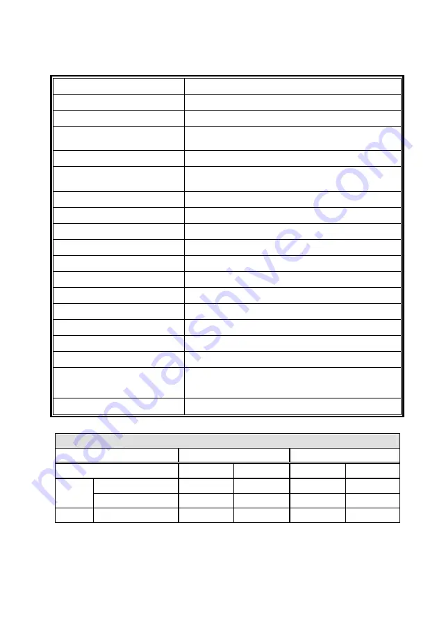
 

LABEL FUNCTION 

JP2, JP3 

PCI-X slot frequency setting 

VIO_J1 

PCI-X slot VIO power setting 

USB1, USB2 

External USB 2.0 connectors from the 
mainboard 

FAN1, FAN2, FAN3, FAN4 Fan connectors 

ATXCTL1 

Backplane to mainboard ATX power control 
connector 

PWR1 

ATX power connector 

12V1


ATX 12V power source connector 

PWRBTN 

External power button connector 

RESET 

External reset button connector 

PWRGD


External power good connector 

SM-BUS


External system management connector 

CN1 

PCIe x16 SDVO control signal connector 

IOPWR 

I/O power connector 

PWR2 

AT +5V power connector 

PWR3, PWR4 

AT +3.3V power connectors 

PCIE1 

PCIe x16 slot 

PCI-X_A1, PCI-X_A2, 

PCI-X_A3, PCI-X_A4 

PCI-X slots 

PCI1, PCI2, PCI3, PCI 4  PCI slots 


JP2, JP3: PCI-X slot frequency setting


 JP2 

JP3 

FREQUENCY/PIN NO.

1 - 2 

2 -3 

1 - 2 

2 - 3


33 MHz 

Short 

Open 

Open 

Short 

PCI 

66 MHz (Default)

Open 

Short 

Short 

Open 

PCI-X  66 MHz (Default)

Open 

Short 

Short 

Open 

Summary of Contents for PXE-12S

Page 1: ... PCI X Slots and Four PCI Slots PXE 12S Quick Installation Guide Version 1 1 November 19 2015 Package List PXE 12S package includes the following items z 1 x PXE 12S PICMG 1 3 backplane z 1 x QIG Copyright 2015 IEI Integration Corp All rights reserved ...

Page 2: ...2 V power 2x4 pin 1 x I O power 2x10 pin 1 x Power button 1x2 pin 1 x Reset button 1x2 pin 1 x Power good 1x2 pin 1 x SMBus 1x2 pin z Dimensions 311 mm x 328 mm Ordering Information z PXE 12S R11 PICMG 1 3 backplane with one PCIe x16 slot four PCI X slots and four PCI slots z RACK 3000G 4U 14 slot full size rack mount chassis z RACK 305G 4U 14 slot full size rack mount chassis z RACK 360G 4U 14 sl...

Page 3: ... button connector RESET External reset button connector PWRGD External power good connector SM BUS External system management connector CN1 PCIe x16 SDVO control signal connector IOPWR I O power connector PWR2 AT 5V power connector PWR3 PWR4 AT 3 3V power connectors PCIE1 PCIe x16 slot PCI X_A1 PCI X_A2 PCI X_A3 PCI X_A4 PCI X slots PCI1 PCI2 PCI3 PCI 4 PCI slots JP2 JP3 PCI X slot frequency setti...

Page 4: ... 2 0 connectors from the mainboard PIN NO DESCRIPTION PIN NO DESCRIPTION 1 USB_VCC 2 GND 3 DATA 4 DATA 5 DATA 6 DATA 7 GND 8 USB_VCC FAN1 FAN2 FAN3 FAN4 Fan connectors PIN NO DESCRIPTION PIN NO DESCRIPTION 1 GND 2 12V 3 NC VIO_J1 PCI X slot VIO power setting OPTIONS DESCRIPTION 5V Short 1 4 2 5 3 6 3 3V Short 7 4 8 5 9 6 Default 9 8 7 3 2 1 ...

Page 5: ...nector PIN NO DESCRIPTION PIN NO DESCRIPTION 1 GND 2 SHB_RST 12V1 ATX 12V power source connector PIN NO DESCRIPTION PIN NO DESCRIPTION 1 GND 2 12V 2 GND 4 12V 3 GND 6 12V 4 GND 8 12V PWR1 ATX powerconnector PIN NO DESCRIPTION PIN NO DESCRIPTION 1 3 3V 13 3 3V 2 3 3V 14 12V 3 GND 15 GND 4 5V 16 PSON 5 GND 17 GND 6 5V 18 GND 7 GND 19 GND 8 PWRGD 20 NC 9 5VSB 21 5V 10 12V 22 5V 11 12V 23 5V 12 3 3V 2...

Page 6: ... 1 GND 2 12V 3 12V 4 GND 5 IPMB_DA 6 5VSB 7 GND 8 GND 9 IPMB_CL 10 5VSB 11 5V 12 PWRGD 13 SMDAT 14 SHB_RST 15 5VSB 16 GND 17 SMCLK 18 PSON 19 3 3V 20 PWRBT CN1 PCIe x16 SDVO control signal connector PIN NO DESCRIPTION PIN NO DESCRIPTION 1 EXP_EN 2 SDVO_CLK 3 SDVO_DAT SM BUS External system management connector PIN NO DESCRIPTION PIN NO DESCRIPTION 1 SMDAT 2 SMCLK ...

Page 7: ...GNT2 AD29 D A B C PCI4 REQ3 GNT3 AD28 A B C D PWR3 PWR4 AT 3 3V power connector PIN NO DESCRIPTION PIN NO DESCRIPTION 1 3 3V 2 3 3V 3 3 3V 4 GND 5 GND 6 GND PCI Express to PCI X routing table SIGNAL REQ GNT IDSEL INTA INTB INTC INTD PIN NO B18 A17 A26 A6 B7 A7 B8 PCI1 REQ0 GNT0 AD28 A B C D PCI2 REQ1 GNT1 AD29 B C D A PCI3 REQ2 GNT2 AD30 C D A B PCI4 REQ3 GNT3 AD31 D A B C ...

Page 8: ...8 Board Layout Jumper and Connector Locations Unit mm ...

Reviews: