WAFER-PV-D5252/D4252/N4552 SBC
Page iii
Copyright
COPYRIGHT NOTICE
The information in this document is subject to change without prior notice in order to
improve reliability, design and function and does not represent a commitment on the part
of the manufacturer.
In no event will the manufacturer be liable for direct, indirect, special, incidental, or
consequential damages arising out of the use or inability to use the product or
documentation, even if advised of the possibility of such damages.
This document contains proprietary information protected by copyright. All rights are
reserved. No part of this manual may be reproduced by any mechanical, electronic, or
other means in any form without prior written permission of the manufacturer.
TRADEMARKS
All registered trademarks and product names mentioned herein are used for identification
purposes only and may be trademarks and/or registered trademarks of their respective
owners.
Summary of Contents for WAFER-PV-D4252
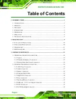
Page 14: ...WAFER PV D5252 D4252 N4552 SBC Page 1 Chapter 1 1 Introduction...
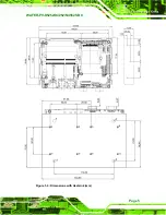
Page 18: ...WAFER PV D5252 D4252 N4552 SBC Page 5 Figure 1 4 Dimensions with Heatsink mm...
Page 22: ...WAFER PV D5252 D4252 N4552 SBC Page 9 Chapter 2 2 Packing List...
Page 26: ...WAFER PV D5252 D4252 N4552 SBC Page 13 Chapter 3 3 Connector Pinouts...
Page 52: ...WAFER PV D5252 D4252 N4552 SBC Page 39 Chapter 4 4 Installation...
Page 76: ...WAFER PV D5252 D4252 N4552 SBC Page 63 Chapter 5 5 BIOS...
Page 104: ...WAFER PV D5252 D4252 N4552 SBC Page 91 Appendix A A BIOS Options...
Page 107: ...WAFER PV D5252 D4252 N4552 SBC Page 94 Appendix B B One Key Recovery...
Page 135: ...WAFER PV D5252 D4252 N4552 SBC Page 122 Appendix C C Terminology...
Page 139: ...WAFER PV D5252 D4252 N4552 SBC Page 126 Appendix D D Hazardous Materials Disclosure...


