WAFER-PV-D5252/D4252/N4552 SBC
Page 14
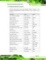
3.1 Peripheral Interface Connectors
Section 3.1.2
shows peripheral interface connector locations.
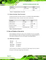
lists all the
peripheral interface connectors seen in
Section 3.1.2
.
3.1.1 Layout
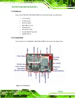
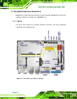
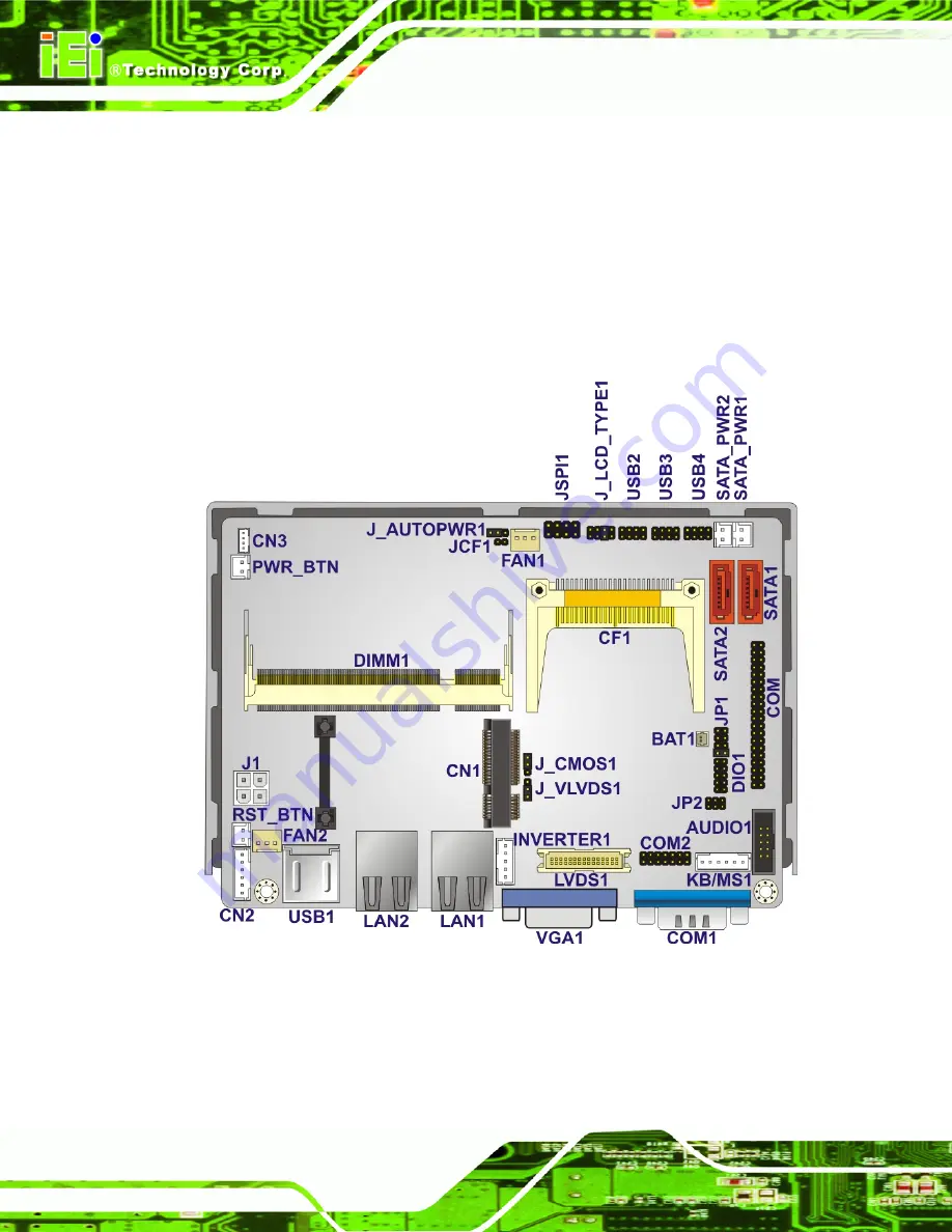
The figure below shows the on-board peripheral connectors, rear panel peripheral
connectors and on-board jumpers.
Figure 3-1: Connector and Jumper Locations
Summary of Contents for WAFER-PV-D4252
Page 14: ...WAFER PV D5252 D4252 N4552 SBC Page 1 Chapter 1 1 Introduction...
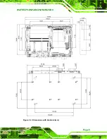
Page 18: ...WAFER PV D5252 D4252 N4552 SBC Page 5 Figure 1 4 Dimensions with Heatsink mm...
Page 22: ...WAFER PV D5252 D4252 N4552 SBC Page 9 Chapter 2 2 Packing List...
Page 26: ...WAFER PV D5252 D4252 N4552 SBC Page 13 Chapter 3 3 Connector Pinouts...
Page 52: ...WAFER PV D5252 D4252 N4552 SBC Page 39 Chapter 4 4 Installation...
Page 76: ...WAFER PV D5252 D4252 N4552 SBC Page 63 Chapter 5 5 BIOS...
Page 104: ...WAFER PV D5252 D4252 N4552 SBC Page 91 Appendix A A BIOS Options...
Page 107: ...WAFER PV D5252 D4252 N4552 SBC Page 94 Appendix B B One Key Recovery...
Page 135: ...WAFER PV D5252 D4252 N4552 SBC Page 122 Appendix C C Terminology...
Page 139: ...WAFER PV D5252 D4252 N4552 SBC Page 126 Appendix D D Hazardous Materials Disclosure...


