WAFER-ULT/ULT2-i1 3.5" SBC
Page 62
4.7.5 LVDS Voltage Selection
WARNING:
Permanent damage to the screen and WAFER-ULT/ULT2-i1 may
occur if the wrong voltage is selected with this jumper. Please refer to
the user guide that came with the monitor to select the correct voltage.
Jumper Label:
JP1
Jumper Type:
3-pin header, p=2 mm
Jumper Settings:
See
Jumper Location:
See
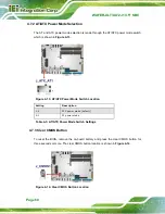
The LVDS voltage selection jumper allows setting the voltage provided to the monitor
connected to the LVDS connector.
Setting
Description
Short 1-2
+3.3V LVDS (Default)
Short 2-3
+5V LVDS
Table 4-5: LVDS Voltage Selection Jumper Settings
Figure 4-16: LVDS Voltage Selection Jumper Location
Summary of Contents for WAFER-ULT-i1
Page 9: ...WAFER ULT ULT2 i1 3 5 SBC Page ix E WATCHDOG TIMER 144 F HAZARDOUS MATERIALS DISCLOSURE 147...
Page 16: ...WAFER ULT ULT2 i1 3 5 SBC Page 1 Chapter 1 1 Introduction...
Page 21: ...WAFER ULT ULT2 i1 3 5 SBC Page 6 Figure 1 3 WAFER ULT ULT2 i1 Dimensions mm...
Page 26: ...WAFER ULT ULT2 i1 3 5 SBC Page 11 Chapter 2 2 Packing List...
Page 31: ...WAFER ULT ULT2 i1 3 5 SBC Page 16 Chapter 3 3 Connectors...
Page 64: ...WAFER ULT ULT2 i1 3 5 SBC Page 49 Chapter 4 4 Installation...
Page 88: ...WAFER ULT ULT2 i1 3 5 SBC Page 73 Chapter 5 5 BIOS...
Page 127: ...WAFER ULT ULT2 i1 3 5 SBC Page 112 6 Software Drivers Chapter 6...
Page 147: ...WAFER ULT ULT2 i1 3 5 SBC Page 132 Appendix A A Regulatory Compliance...
Page 149: ...WAFER ULT ULT2 i1 3 5 SBC Page 134 Appendix B B BIOS Options...
Page 152: ...WAFER ULT ULT2 i1 3 5 SBC Page 137 Appendix C C Terminology...
Page 156: ...WAFER ULT ULT2 i1 3 5 SBC Page 141 Appendix D D Digital I O Interface...
Page 159: ...WAFER ULT ULT2 i1 3 5 SBC Page 144 Appendix E E Watchdog Timer...
Page 162: ...WAFER ULT ULT2 i1 3 5 SBC Page 147 Appendix F F Hazardous Materials Disclosure...


