background image


CPU_45B-V1 


CPU Board XMC4500 SDRAM 


Production Data 

Board User's Manual 

34 

Revision 1.0, 2013-02-20 


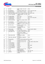
26 

BK-885 

Battery Holder, 12mm Coin 
Cell 

X402 

27 

BLM18PG600 

Ferrite Bead, 0603, Murata 

L201, L300, L301, L500 

28 

ESD8V0L2B-03L 

Diode, TSLP-3-1, Infineon 

V201, V500 

29 

HSEC8_MATING-CARD  Connector, Edgecard, Samtec  X200, X201, X202 

30 

IFX1763_PADNOP 

Voltage Regulator, 3.3V LDO, 
Infineon 

U401 

31 

LED-GE/D/0603 

LED, yellow 

V300, V301 

32 

LED-GN/D/0603 

LED, green 

V401, V402, V403, V502 

33 

LED-RT/D/0603 

LED, red 

V407 

34 

IS42S16400F-7BL 

Synchronous Dynamic RAM, 
ISSI 

U430 

35 

NC7WZ07P6X 

IC, Dual Buffer OD, SC70-6 

U501 

36 

POTI/10K/VERT 

Potentiometer, K09K1130A8G, 
ALPS 

R300 

37 

S2*10/1.27SO 

Connector, FTSH-110-01-L-
DV-K-P, Samtec 

X400 

38 

S25FL032P0XMFI01 

IC, qSPI Flash Memory, 
SPANSION 

U302 

39 

TMPS2-SMD 

Switch, tactile 

SW400, SW401, SW402 

40 

TPS2051BDBV 

IC, Power Switch, SOT23-5 

U200 

41 

XCTX 

Connector, FTSH-105-01-LM-
DV-K, w/o pin 7, Samtec 
Connector, FLE-103-01-G-DV, 
Samtec 

X401 

42 

XMC4200_QFN48 

IC, XMC4200, QFN48, 
Infineon 

U500 

43 

XMC4500_LFBGA144 

IC, XMC4500, LFBGA144, 
Infineon 

U300 

44 

ZX62-AB-5PA 

Connector, Micro-USB, Hirose  X203, X500 

45 

no ass. 

Pinheader, 4-pin, 0.1" TH 

X501 

46 

no ass. 

Pinheader, 1-pin, 0.1" TH 

TP404, TP405, TP406, TP407 

47 

no ass./0R/0603 

Resistor 

R417 

48 

no ass./4k7/0402 

Resistor 

R427 

49 

no ass./10k/0402 

Resistor 

R205, R413 

50 

no ass./10nF/0402 

Capacitor 

C503 

51 

no ass./33R/0402 

Resistor 

R404, R410 

52 

no ass. 

Pinheader, 3-pin, 0.1" TH, 
Hitex PowerScale 

JP300 

53 

no ass. 

Solder Bridge (open) 

SJ1, SJ2, SJ3 

54 

0R/0402 

Solder Bridge (closed by 
resistor) 

SJ4, SJ5 


Summary of Contents for CPU_45B-V1

Page 1: ...Microcontroller Hexagon Application Kit For XMC4000 Family Board User s Manual Revision 1 0 2013 02 20 CPU_45B V1 CPU Board XMC4500 SDRAM ...

Page 2: ...ery terms and conditions and prices please contact the nearest Infineon Technologies Office www infineon com Warnings Due to technical requirements components may contain dangerous substances For information on the types in question please contact the nearest Infineon Technologies Office Infineon Technologies components may be used in life support devices or systems only with the express written a...

Page 3: ...cos AG FLEXGO of Microsoft Corporation FlexRay is licensed by FlexRay Consortium HYPERTERMINAL of Hilgraeve Incorporated IEC of Commission Electrotechnique Internationale IrDA of Infrared Data Association Corporation ISO of INTERNATIONAL ORGANIZATION FOR STANDARDIZATION MATLAB of MathWorks Inc MAXIM of Maxim Integrated Products Inc MICROTEC NUCLEUS of Mentor Graphics Corporation Mifare of NXP MIPI...

Page 4: ...ion 13 2 5 Debug Interface 14 2 5 1 On board USB Debugger 15 2 5 2 Cortex Debug Connector 10 pin 16 2 5 3 Cortex Debug ETM Connector 20 pin 17 2 6 Serial Flash Memory 19 2 7 SDRAM 20 2 8 USB 20 2 9 RTC 22 2 10 User LEDs and User Button 23 2 11 Potentiometer 23 2 12 Satellite Connectors 24 2 12 1 COM Connector 25 2 12 2 HMI Connector 26 2 12 3 ACT Satellite Connector 27 3 Production Data 27 3 1 Sch...

Page 5: ...Connector 10 pin Layout 17 Figure 13 Cortex Debug ETM Connector 20 pin 17 Figure 14 Cortex Debug ETM Connector 20 pin Layout 18 Figure 15 Quad SPI Flash Interface 19 Figure 16 SDRAM Interface 20 Figure 17 USB Connector 20 Figure 18 USB power generation Host OTG mode 21 Figure 19 Battery Holder for Coin Cells 22 Figure 20 XMC4500 Power Domains and Real Time Clock 22 Figure 21 User LEDs and User But...

Page 6: ...s LEDs 10 Table 2 Power Measurement 11 Table 3 Boot Options Settings 13 Table 4 Cortex Debug Connector 10 Pin 16 Table 5 Cortex Debug ETM Connector 20 Pin 18 Table 6 Quad SPI Signals 19 Table 7 USB micro AB connector Pinout 21 Table 8 User LEDs 23 Table 9 User Buttons 23 Table 10 Potentiometer 23 Table 11 BOM of CPU_45B V1 Board 33 ...

Page 7: ...n designed to work with the General Purpose Motor Drive Card MOT_GPDLV For this purpose please use the CPU boards CPU_45A CPU_44A or CPU_42A The focus is safe operation under evaluation conditions The board is neither cost nor size optimized and does not serve as a reference design 1 1 Key Features The CPU_45B V1 board is equipped with the following features XMC4500 ARM Cortex M4 based Microcontro...

Page 8: ...onnectors Variable resistor POTI connected to GPIO P14 1 USB On The Go Connector Micro USB On board Debugger via USB connector Micro USB Figure 1 CPU_45B V1 Board Block Diagram Block_Diag emf EE XMC4500 LFBGA144 EE 2xISOFACE QSPI I2C I2C CAN CAN1 CAPCOM ENCODER DSMOD SENSOR OPAMP TOUCH U2C1 CPU Board XMC4500 SDRAM CPU_45B V1 U1C1 2xCS ETH ETH RMII USB OTG USB CCU 4 8 POSIF DSD DAC ADC GPIO reset Q...

Page 9: ...rrent required exceeds 500 mA then the board needs to be powered by a satellite card which supports external power supply like e g AUT_ISO V1 MOT_GPDLV V2 COM_ETH V1 The typical current drawn by the CPU board without any satellite cards connected is about 220 mA 5V For powering the board through an USB interface connect the USB cable provided with the kit to either of the Micro USB connector on bo...

Page 10: ...V402 VDD5USB 5 V ON if powered by USB OTG connector X203 OFF in all other supply cases V403 VDD3 3 3 3 V Must always be ON Figure 4 Block Diagram Of Power Supply Power emf USB OTG Debug USB Power indicating LEDs IFX1763 3 3V Linear Voltage Regulator PowerScale Probe CPU Board XMC4500 SDRAM CPU_45B V1 ACT Sat Connector COM Sat Connector HMI Sat Connector Debug USB VDD5USB Lin Voltage Regulator IFX1...

Page 11: ...to measure the power consumption of the XMC4500 device Table 2 Power Measurement Jumper Function Description JP300 PowerScale A Hitex PowerScale probe can be connected for current sensing the VDD3 3 CPU power source Default pos 1 2 closed Note On the PCB there is a shorting trace between pin 1 2 This trace has to be cut first before using PowerScale Pin 3 is GND ...

Page 12: ...connected to either Cortex Debug connector X400 or X401 The RESET signal is routed to all satellite connectors The reset circuit includes a red LED V407 to indicate the reset status The Reset LED V407 will be ON during active reset state and will be OFF if reset is not active Be aware that PORST is a bidirectional reset pin of the XMC4000 family which can also be pulled low by the XMC4000 device i...

Page 13: ...scillations during operations For the RTC clock a separate external 32 768 kHz crystal is used on board Figure 7 Clock Generation Circuit 2 4 Boot Option During power on reset the XMC4500 latches the dip switch SW300 settings via the TCK and the TMS pin Based on the values latched different boot options are possible Table 3 Boot Options Settings BSL TMS CAN UART TCK Boot Option OFF 1 UART 0 Normal...

Page 14: ... because the GPIO P0 7 where the required TDI function is mapped to also is used by the on board SDRAM device and various Actuator boards connected to the ACT satellite connector Attention It is strongly recommended not to use JTAG debug mode especially if satellites boards are connected which uses the GPIO 0 7 For the same reason also do not use the on board debugger in JTAG mode If you want to u...

Page 15: ...t J Link driver see Figure 9 2 Serial Wire Viewer operation does not work during use of the on board SDRAM Figure 9 Installation of Serial Port Driver The on board debugger can be accessed through the Debug USB connector shown in Figure 10 The Debug LED V502 shows the status during debugging Figure 10 On Board USB Debugger When using an external debugger connected to the 10pin 20pin Cortex Debug C...

Page 16: ...nnected from the Cortex Debug Connectors by a not assembled resistor R410 because the pin P0 7 can be used by the on board SDRAM by Actuator boards connected to the ACT satellite connector and by boards connected to the COM satellite connector Figure 11 Cortex Debug Connector 10 pin Table 4 Cortex Debug Connector 10 Pin Pin No Signal Name Serial Wire Debug JTAG Debug 1 VCC 3 3 V 3 3 V 2 SWDIO TMS ...

Page 17: ...nyway the resistor R404 needs to be assembled JTAG operation additionally would require the TDI P0 7 signal By default the TDI signal is disconnected from the Cortex Debug Connectors by a not assembled resistor R410 because the pin P0 7 can be used by the on board SDRAM by Actuator boards connected to the ACT satellite connector and by boards connected to the COM satellite connector Figure 13 Cort...

Page 18: ...t Data OUT 7 KEY KEY KEY 8 NC TDI Not connected Test Data IN 9 GNDDetect Ground Detect Ground Detect 10 nRESET Reset Active Low Reset Active Low 11 GND TgtPwr Cap Ground Ground 12 TRACECLK Trace Clock Trace Clock 13 GND TgtPwr Cap Ground Ground 14 TRACEDATA 0 Trace Data 0 Trace Data 0 15 GND Ground Ground 16 TRACEDATA 1 Trace Data 1 Trace Data 1 17 GND Ground Ground 18 TRACEDATA 2 Trace Data 2 Tra...

Page 19: ...rfaced to XMC4500 through a SPI interface The SPI interface can be configured as single dual or quad SPI Table 6 Quad SPI Signals Pin No Signal Name Signal Description P0 13 CLK Clock P3 3 CS Active Low Chip Select P3 15 DI Data Input of Flash MTSR P3 14 DO Data Output of Flash MRST P0 14 Data I O Data Input Output P0 15 Data I O Data Input Output Figure 15 Quad SPI Flash Interface ...

Page 20: ...ation system is higher than 500 mA power from an external source through satellite cards shall be used Note Some PCs notebooks or hubs have a weak USB supply which is not sufficient for proper supply In this case use an external 5 Volt power supply or a powered USB hub Figure 17 USB Connector The USB ID pin of the USB connector is connected to the port pin P15 2 of the XMC4500 This pin must be pol...

Page 21: ...e CPU_45B V1 board is capable of supplying power to the connected device e g USB mouse The board has a power switch which is controlled by the USB BUSDRIVE signal of XMC4500 USB BUSDRIVE is mapped to Port P0 1 active high In the Host OTG mode a low active FAULT signal indicates to XMC4500 via HIB_IO_0 signal if more than 500 mA current is drawn by the external device HIB_IO_0 signal is used as gen...

Page 22: ...ery Holder for Coin Cells The Real Time Clock RTC is located in the hibernate domain The XMC4500 uses the HIB_IO_1 signal active low to shutdown the external LDO voltage regulator which generates VDD3 3 core domain Even if the Core Domain is not powered the Hibernate Domain will operate if VBAT is available The RTC keeps running as long as the Hibernate Domain is powered via the auxiliary supply V...

Page 23: ...1 Two User Buttons SW401 and SW402 are connected to P5 10 and P0 10 of XMC4500 Table 9 User Buttons Button Connected to Port Pin Button1 SW401 GPIO P5 10 Button2 SW402 GPIO P0 10 Figure 21 User LEDs and User Buttons 2 11 Potentiometer The CPU_45B V1 board provides a potentiometer for ease of use and testing of the on chip analog to digital converter The potentiometer is connected to the analog inp...

Page 24: ...on by satellite cards COM satellite connector Communication HMI satellite connector Human Machine Interface ACT satellite connector Actuator Note Satellite cards shall be connected to their matching connectors only For e g COM satellite cards shall be connected to COM satellite connector only Figure 22 Satellite Connectors Satt_Conn emf ACT Satellite Connector HMI Satellite Connector COM Satellite...

Page 25: ...14 16 18 20 22 24 26 28 30 32 34 36 38 40 42 44 46 48 50 52 54 56 58 60 62 64 66 68 70 72 74 76 78 80 Connector 1 3 5 7 9 11 13 15 17 19 21 23 25 27 29 31 33 35 37 39 41 43 45 47 49 51 53 55 57 59 61 63 65 67 69 71 73 75 77 79 Function GND qSPI_SCLK qSPI_CS qSPI_CS RSVD RSVD ETH_RMII ETH_RMII ETH_RMII ETH_RMII ETH_RMII RSVD ASC_DIR ASC_RXD ASC_TXD SPI_CSC0 SPI_CSC1 SPI_CSC2 I2C_SDA COM_GPIO1 COM_G...

Page 26: ...C18 RSVD RSVD TP7 TP6 TP5 TP4 TP3 TP2 TP1 TP0 GND Satellite 2 4 6 8 10 12 14 16 18 20 22 24 26 28 30 32 34 36 38 40 42 44 46 48 50 52 54 56 58 60 62 64 66 68 70 72 74 76 78 80 Connector 1 3 5 7 9 11 13 15 17 19 21 23 25 27 29 31 33 35 37 39 41 43 45 47 49 51 53 55 57 59 61 63 65 67 69 71 73 75 77 79 Function GND MMC_CLK MMC_DATA1 MMC_DATA3 MMC_DATA5 MMC_DATA7 MMC_BUSPOW MMC_nSDCD RSVD RSVD RSVD Au...

Page 27: ...1 73 75 77 79 Function GND PIF1IN0 PIF1IN1 PIF1IN2 PWMN PWMP DSDCLK0 DSDCLK1 RSVD CC_IN3 CC_IN4 CC_IN5 TRAP_A TRAP_B TRAP_X SPI_CSA0 SPI_CSA1 SPI_CSA2 I2C_SDA ACT_GPIO1 ACT_GPIO0 VDD5 VDD5 AGND DAC0 ADC1 ADC3 ORC0 ADC5 ORC2 ADC7 ADC9 ADC11 ADC13 PWMB0_H PWMB0_L PWMB1_H PWMB1_L PWMB2_H PWMB2_L PWMX2 PWMX3 GND XMC Function GND nc nc nc DSD_PWMN DSD_PWMP nc DSD_MCLK3 nc nc nc nc nc nc nc U2C0 SELO3 U...

Page 28: ...2 43 43 44 44 45 45 46 46 47 47 48 48 49 49 50 50 51 51 52 52 53 53 54 54 55 55 56 56 57 57 58 58 59 59 60 60 61 61 62 62 63 63 64 64 65 65 66 66 67 67 68 68 69 69 70 70 71 71 72 72 73 73 74 74 75 75 76 76 77 77 78 78 79 79 80 80 X200 1 1 2 2 3 3 4 4 5 5 6 6 7 7 8 8 9 9 10 10 11 11 12 12 13 13 14 14 15 15 16 16 17 17 18 18 19 19 20 20 21 21 22 22 23 23 24 24 25 25 26 26 27 27 28 28 29 29 30 30 31 ...

Page 29: ...P0 8 A8 P0 9 D4 P0 10 B4 P0 11 E5 P0 12 D5 P0 13 C5 P0 14 E6 P0 15 C6 P1 0 D9 P1 1 E9 P1 2 C11 P1 3 C12 P1 4 C10 P1 5 D10 P1 6 B9 P1 7 B10 P1 8 A10 P1 9 B11 P1 10 D12 P1 11 D11 P1 12 E11 P1 13 E12 P1 14 E10 P1 15 G12 P2 0 J11 P2 1 K12 P2 2 K11 P2 3 L11 P2 4 L10 P2 5 M10 P2 6 J9 P2 7 K9 P2 8 L9 P2 9 M9 P2 10 L8 P2 11 M8 P2 12 L7 P2 13 M7 P2 14 K7 P2 15 J6 P3 0 C1 P3 1 B2 P3 2 B3 P3 3 F7 P3 4 E7 P3 ...

Page 30: ...1 SW401 P P1 S S1 SW402 1 TP404 1 TP405 1 TP406 1 TP407 BYP 4 EN 5 EXP 9 GND 3 GND 6 GND 7 IN 8 OUT 1 SENSE ADJ 2 U401 A0 H7 A1 H8 A2 J8 A3 J7 A4 J3 A5 J2 A6 H3 A7 H2 A8 H1 A9 G3 A10 H9 A11 G2 BA0 G7 BA1 G8 CAS F7 CKE F3 CLK F2 CS G9 DQ0 A8 DQ1 B9 DQ2 B8 DQ3 C9 DQ4 C8 DQ5 D9 DQ6 D8 DQ7 E9 DQ8 E1 DQ9 D2 DQ10 D1 DQ11 C2 DQ12 C1 DQ13 B2 DQ14 B1 DQ15 A2 LDQM E8 NC E2 NC G1 RAS F8 UDQM F1 WE F9 U430A V...

Page 31: ...01 1 2 3 V500 A C V501 V502 1 2 3 4 5 X500C X500S 1 2 3 4 X501 CPU_45B V1 18 10 2012 14 43 12 5 5 Sheet A B C D E 1 2 3 4 5 6 7 8 A B C D E 1 2 3 4 5 6 7 8 Legal Disclaimer The information given in this document shall in no event be regarded as a guarantee of conditions or characteristics With respect to any examples or hints given herein any typical values stated herein and or any information reg...

Page 32: ... C406 C407 C413 C414 C415 C416 C417 C 4 3 0 C 4 3 1 C 4 3 2 C433 C 4 3 4 C 4 3 5 C 4 3 6 C500 C501 C502 C503 C504 C505 C506 C507 C508 C509 C510 C511 C512 JP300 L201 L 3 0 0 L 3 0 1 L500 Q 3 0 1 Q 3 0 2 Q404 Q500 R200 R202 R203 R204 R205 R206 R207 R300 R301 R 3 0 2 R303 R 3 0 4 R305 R306 R307 R 3 0 9 R 3 1 0 R 3 1 3 R400 R401 R402 R403 R404 R405 R406 R407 R408 R410 R413 R414 R415 R416 R417 R419 R42...

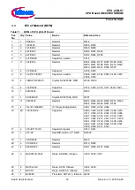
Page 33: ...6 15pF 0402 Capacitor C312 C315 C316 C317 C500 C501 12 1 22R 0402 Resistor R432 13 1 32 768KHZ Crystal NX3215SA NDK Q301 14 11 33R 0402 Resistor R202 R203 R402 R403 R421 R423 R424 R425 R426 R501 R502 15 4 74LVC1G66DCK IC Single Analog Switch U301 U303 U304 U306 16 40 100nF 0402 Capacitor C200 C202 C204 C205 C208 C210 C211 C300 C301 C302 C305 C306 C307 C309 C310 C311 C318 C319 C321 C322 C413 C416 C...

Page 34: ...r FTSH 110 01 L DV K P Samtec X400 38 1 S25FL032P0XMFI01 IC qSPI Flash Memory SPANSION U302 39 3 TMPS2 SMD Switch tactile SW400 SW401 SW402 40 1 TPS2051BDBV IC Power Switch SOT23 5 U200 41 1 XE3K_DM2 CTX Connector FTSH 105 01 LM DV K w o pin 7 Samtec Connector FLE 103 01 G DV Samtec X401 42 1 XMC4200_QFN48 IC XMC4200 QFN48 Infineon U500 43 1 XMC4500_LFBGA144 IC XMC4500 LFBGA144 Infineon U300 44 2 ...

Page 35: ...w w w i n f i n e o n c o m Published by Infineon Technologies AG ...

Reviews: