CY8CKIT-064S0S2-4343W PSoC 64 Standard Secure – AWS Wi-Fi BT Pioneer Kit Guide, Doc. # 002-30680 Rev. *B
37
Hardware
4.2.5.1
Voltage regulators
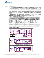
The power supply system is designed for the voltage configurations listed in
. Some
configurations achievable on this kit are outside the operating range for the device. However, it is not
possible to achieve all applicable configurations by changing jumper positions but rather requires re-
work of respective 0-ohm resistors.
VDDIO_WL and VDDIO2_MCU must be at the same voltage since they power the SDIO interface
between PSoC 64 MCU and CYW4343W. Hence both are supplied by the VCC_VDDIO2_IN
domain.
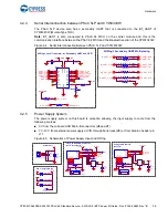
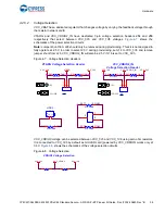
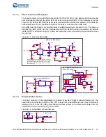
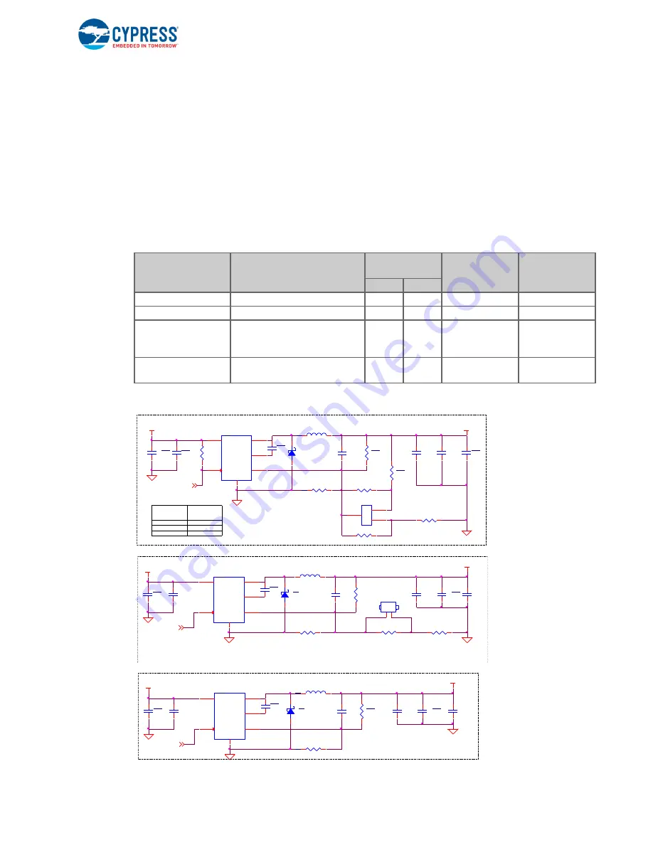
Three buck regulators
U15
,
U13
and
U7
are used to achieve 1.8 V, 3.3 V and 3.6 V outputs
respectively.
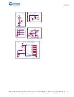
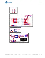
shows the schematics of the voltage regulator circuits.
VCC_VBAT
VBAT_WL
3.2
4.2
3.6V, 3.3V
J9
VCC_VDDIO2_IN
VDDIO2_MCU, VDDIO_WL
1.71
3.63
1.8V, 3.3V
J16
VTARG
VDDD_MCU, VDDIO1_MCU,
VDDA_MCU, VDD_NS_MCU,
VBACKUP_MCU
1.7
3.6
1.8, 2.5, 3.3V
J14, J26
VCC_VDDIO0
VDDIO0_MCU
1.7
3.6
1.8, 2.5, 3.3V
None
(uses 0 Ohms)
Figure 4-6. Voltage Regulators
Table 4-1. Operating voltage ranges of domains
Voltage Domain
Carrier Module (MOD1)
Power Pins powered by the
domain
Operating
Voltage
Voltage
Configuration
applicable in kit
Voltage
Selection
Header
Min (V) Max (V)
D5
PMEG3020BEP
R171
0 OHM
No Load
R172
0 OHM
No Load
C74
47pF
50V
R72
100K
1%
C79
22uF
25V
AOZ1280CI
U7
GN
D
2
LX
6
IN
5
FB
3
EN
4
BST
1
R73
27.4K
1%
C45
10nF
50V
Voltage (V)
J9 Jumper
Not Present
3.3
1.8
1-2
2-3
3.6
B_KP_PMIC_EN
Note: 1.8V is not a valid
operating voltage on this kit.
C42
10uF
25V
J9
1
2
3
C41
22uF
25V
VCC_IN
C43
0.1uF
16V
3.6V 1A
VBAT Voltage Regulator
VCC_VBAT
L1
4.7uH
R69
40.2K
1%
R70
13K
1%
C46
0.1uF
16V
R71
100K
C35
22uF
25V
VCC_IN
C37
0.1uF
16V
VCC_3V3
3.3V 600mA
3.3V Voltage Regulator
L2
4.7uH
C40
0.1uF
16V
B_KP_PMIC_EN
R177
47K
1%
J26
HDR2
1
2
D6
PMEG3020BEP
C75
47pF
50V
C80
10uF
25V
AOZ1280CI
U13
GN
D
2
LX
6
IN
5
FB
3
EN
4
BST
1
C39
10nF
50V
R180
0 OHM
No Load
R181
100K
1%
R182
100K
1%
Note: Regulator output w ill be
3.3V w hen J26 jumper is loaded
and 2.5V w hen removed.
Note: 2.5V configuration is only to be used w hile
eFuse programming. Normal operation is
supported only in 3.3V configuration.
C36
10uF
25V
D7
PMEG3020BEP
C76
47pF
50V
C81
10uF
25V
AOZ1280CI
U15
GN
D
2
LX
6
IN
5
FB
3
EN
4
BST
1
C51
10nF
50V
C47
22uF
25V
VCC_IN
C49
0.1uF
16V
VCC_1V8
L3
4.7uH
1.8V 600mA
1.8V Voltage Regulator
R77
40.2K
1%
R78
32.4K
1%
C52
0.1uF
16V
B_KP_PMIC_EN
C48
10uF
25V


