Data Sheet
51
Rev. 1.00
2017-07-31
TLE9262BQXV33
External Voltage Regulator 3
8
External Voltage Regulator 3
8.1
Block Description
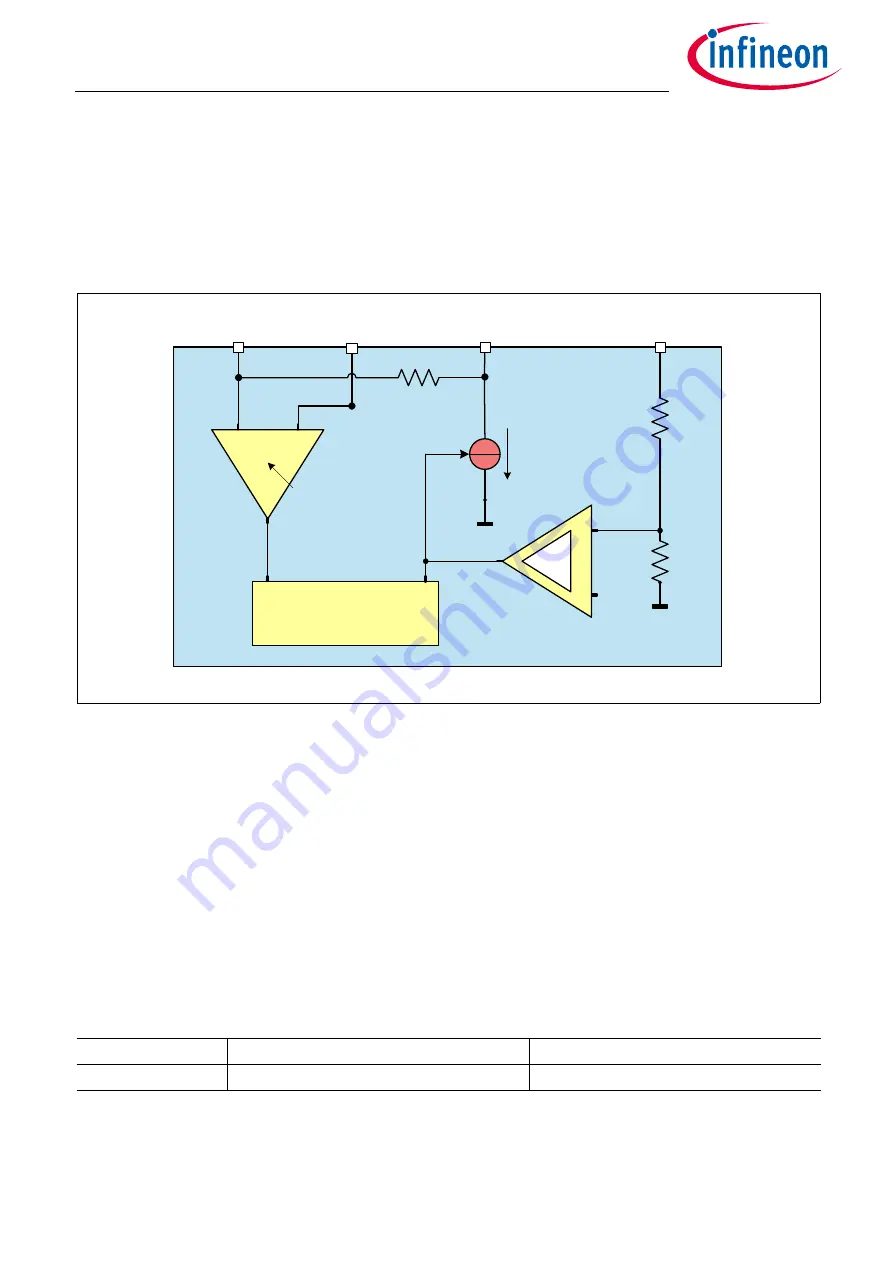
Figure 17 Functional Block Diagram
Functional Features
•
Low-drop voltage regulator with external PNP transistor (up to 350mA with 470m
Ω
shunt resistor)
•
Four high-voltage pins are used: VS, VCC3B, VCC3SH, VCC3REF
• Configurable as stand-alone regulator (3.3V or 1.8V output voltage selectable via SPI) or in load-sharing
mode with VCC1 (3.3V output voltage)
•
≥
4.7µF ceramic capacitor at output voltage for stability, with ESR < 150m
Ω
@ f = 10 kHz to achieve the
voltage regulator control loop stability based on the safe phase margin (bode diagram).
• Overcurrent limitation with external shunt in stand-alone configuration
•
Adjustable load current sharing ratio between VCC1 and VCC3 for load-sharing configuration
• Undervoltage shutdown in stand-alone configuration only
Table 11
1)
External Voltage Regulator Configurations depending on VCC1 output voltage
1) This settings are valid only for the VCC3 stand-alone configuration. The bit
VCC3_ V_CFG
is ignored for VCC3 load
sharing configuration
VCC1 configuration VCC3 voltage for
VCC3_ V_CFG
= 0
VCC3 voltage for
VCC3_ V_CFG
= 1
VCC1 = 3.3V
VCC3 = 3.3V
VCC3 = 1.8V
R
BE
V
S
- V
CC3shunt
> V
shunt_threshold
V
REF
State Machine
+
-
I
CC3base
VCC3REF
VCC3B
VCC3SH
VS


