Data Sheet
84
Rev. 1.00
2017-07-31
TLE9262BQXV33
LIN Transceiver
11.2.5
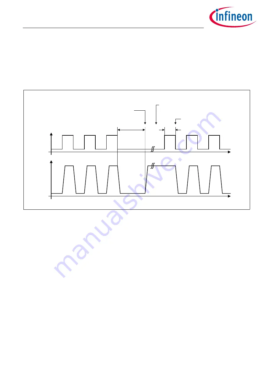
TXD Time-out Feature
If the TXD signal is dominant for the time t >t
TxD_LIN _TO
, the TXD time-out function deactivates the LIN
transmitter output stage temporarily. The transceiver remains in recessive state. The TXD time-out functions
prevents the LIN bus from being blocked by a permanent LOW signal on the TXD pin, caused by a failure. The
failure is stored in the SPI flag
LIN1_FAIL
. The LIN transmitter stage is activated again after the dominant
time-out condition is removed. The transceiver configuration stays unchanged.
Figure 35 TXD Time-Out Function
11.2.6
Bus Dominant Clamping
If the LIN bus signal is dominant for a time
t
>
t
BUS_LIN_TO
in LIN Normal and Receive Only Mode, then a bus
dominant clamping is detected and the SPI bit
LIN1_FAIL
is set. The transceiver configuration stays
unchanged.
11.2.7
Undervoltage Detection
In case the supply voltage is dropping below the VSHS undervoltage detection threshold (VSHS < V
SHS,UVD
), the
TLE9262BQXV33 disables the output and receiver stages. If the power supply reaches a higher level than the
undervoltage detection threshold (VSHS > V
SHS,UVD
), the TLE9262BQXV33 continues with normal operation.
The transceiver configuration stays unchanged.
TxD
LIN
t
torec
t
timeout
Normal Communication
Normal Communication
TxD Time-Out due to
microcontroller error
Release after TxD
Time-out
Recovery of the
microcontroller error
t
t


