background image

Jumpers on the PI-6582V 


17 


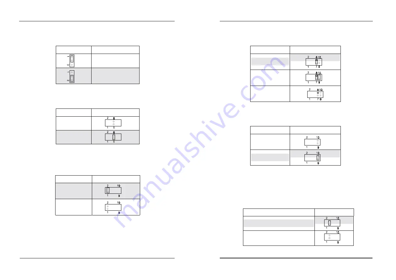
3.3  VGA Flat panel SHF_CLK signal setting (JP15) 


JP15 Singal 


SHF_CLK inverted 


Normal 


3.4  On-board Flash/RAM disk enable/disable (JP13 pin5-6) 


Flash/RAM disk 

JP13 pin 5-6 

Enable 


Disable 


3.5  Flash/RAM disk & watchdog Base port settings    (JP13 

pin1-2) 


I/O Base port 

JP13 pin1-2 

536H - 537H 


636H - 637H 


Jumpers on the PI-6582V 
 

18 
 

3.6  Device setting on the extended socket (M1) (JP13 pin7-8) 


Device type 

JP13 pin7-8 

FLASH 


SRAM 


DiskOnChip 


3.7  DiskOnChip enable/disable setting (JP13 pin9-10) 


DiskOnChip JP13 

pin9-10 

Enable 


Disable 


Note:   1. The socket called “M1” can accept normal memory device (such as SST,   
              ATMEL Flash or SRAM) or DiskOnChip Flash chip by setting jumper JP13   
              pin 9-10 

3.8  On-board Flash/RAM disk address setting (JP13 pin 3-4) 


On board flash disk Memory address 

JP13    pin3-4 

D0000H-D5FFFH 


D8000H-DDFFFH 


Summary of Contents for PI-6582V

Page 1: ...n and dosed not represent a commitment on the part of the manufacturer No part of this manual may be reproduced copied or transmitted in any form without the prior written permission of manufacturer A...

Page 2: ...Pin assignments of connectors 20 0 2 0 2 0 2 0 2 0 2 3 0 2 4 0 2 0 2 0 2 01 2 0 2 8 0 2 0 2 Introductions 4 0 2 57 A 0 6 5 2 8 6 5 How to use on board Flash disk 31 8 3 3 8 8 8 6 How to use DiskOnChip...

Page 3: ...socket that can accept SRAM Flash device or DiskOnChip DOC Flash Disk for embedded application User can use any DOS command without any extra software utility The DOC currently is available from 2MB t...

Page 4: ...two USB ports for future expansion Introductions 8 VGA Display Built in PCI Bus VGA controller C T 65550 Panel support TFT STN EL Mono LCD High performance Flat Panel CRT GUI accelerator 64 bit graph...

Page 5: ...Introductions 9 1 5 P C B layout Introductions 10 1 6 P C B dimension...

Page 6: ...ltage selector JP11 JP12 Short open short open Vio Vcore 5 6 7 8 1 2 3 4 3 4 1 2 5 6 3 3V 3 3V 1 2 3 4 5 6 7 8 1 2 3 4 5 6 3 3V 2 8V 1 2 3 4 5 6 7 8 5 6 1 2 3 4 3 3V 3 5V 1 2 3 4 5 6 7 8 None 1 2 3 4...

Page 7: ...AMD K6 2 300 AMD K6 2 333 Installations 14 Cyrix CPU installation CPU type Internal Clock JP2 External clock JP4 Vio JP11 Vcore JP12 Cyrix 6X86 P120 100MHz Cyrix 6X86 P133 110MHz Cyrix 6X86 P150 120MH...

Page 8: ...the SIMM sockets Memory configuration SIMM1 SIMM2 Total memory 4MB 2 8MB 8MB 2 16MB 16MB 2 32MB 32MB 2 64MB 64MB 2 128MB Jumpers on the PI 6582V 16 3 Jumpers on the PI 6582V 3 1 Battery backup for CMO...

Page 9: ...637H Jumpers on the PI 6582V 18 3 6 Device setting on the extended socket M1 JP13 pin7 8 Device type JP13 pin7 8 FLASH SRAM DiskOnChip 3 7 DiskOnChip enable disable setting JP13 pin9 10 DiskOnChip JP...

Page 10: ...ble 3 11 Watch dog timer time base settings There are two time bases for watch dog timer 1 sec or 10 sec by setting jumper JP14 pin 3 4 5 6 Watch dog time base JP14 pin 3 4 5 6 1 sec 10 sec Pin assign...

Page 11: ...1 GND 2 2V DC 3 GND 4 6 PS 2 mouse connector CN5 Pin No Signal 1 MS_data 2 N C 3 GND 4 5V DC 5 MS_clk 6 N C Pin assignments of connectors 22 4 7 Keyboard connector CN6 Pin No Signal 1 KB_data 2 N C 3...

Page 12: ...Wite enable 26 Track 0 28 write protect 30 Read data 32 Select head 34 Disk change Pin assignments of connectors 24 4 12 Hard disk connector CN2 Pin No Description Pin No Description 1 RST 2 Ground 3...

Page 13: ...of connectors 26 4 14 COM port connectors CN20 connectors has two functions It acts as COM2 4 port connector for PI 6582 and acts as VGA output connector For PI 6582V COM 1 3 port CN9 COM 1 3 Signal 1...

Page 14: ...Pin No Function 1 GND 2 GND 3 SHF_CLK 4 M 5 HSYNC LP 6 VSYNC FLM 7 P0 8 P1 9 P2 10 P3 11 P4 12 P5 13 P6 14 P7 15 P8 16 P9 17 P10 18 P11 19 P12 20 P13 21 P14 22 P15 23 P16 24 P17 25 P18 26 P19 27 P20 2...

Page 15: ...ACK2 A11 BAEN A27 SA4 B11 SMWR B27 TC A12 SA19 A28 SA3 B12 SMRD B28 BALE A13 SA18 A29 SA2 B13 IOW B29 VCC A14 SA17 A30 SA1 B14 IOR B30 OSC A15 SA16 A31 SA0 B15 DACK3 B31 GND A16 SA15 A32 GND B16 DRQ3...

Page 16: ...JP13 pin 5 6 and pin 9 10 are used to enable or disable disk JP13 pin 3 4 is used to set the memory address occupied by disk JP13 pin 7 8 is used to set device type inserted on the socket M1 5 3 Soli...

Page 17: ...ed How to use on board Flash disk 34 Auto detect and boot from Disk A Enabled If system files IO SYS SMDOS SYS existed in Floppy disk A the system will automatically boot form disk A Disabled Normal b...

Page 18: ...SRAM is first time installed into extended socket labeled M1 and set to be secondary disk alone The FORMAT process is necessary before usage C FORMAT Secondary disk name The primary disk size 1 7MB Se...

Page 19: ...isk Step 6 Creat Autoexec bat file in disk A and modify the first line in autoexec bat file to have Diskswap exe command Step 7 Copy DISKSWAP EXE file to disk A from provided utility diskette Step 8 r...

Page 20: ...e No CX Sector No AL Sectors Writes One Sector to memory device 0 1 2 0 1 2 1 2 ES BX Soruce buffer pointer Exit Carry 1 Carry 0 data writing error completed On board Flash RAM disk BIOS function call...

Page 21: ...r xr h ah 2 Function call no in AH xr h dl device_no 0xff Device No in DL xr x cx sector_no Sector No in CX On board Flash RAM disk BIOS function calls 42 xr h al sectors Sectors in AL xr x bx FP_OFF...

Page 22: ...tch dog timer can be enabled disabled by setting jumper JP14 pin 1 2 Watch dog timer JP14 pin 1 2 Enable Watch dog timer time base settings There are two time bases for watch dog timer 1 sec or 10 sec...

Page 23: ...diskette include dos h include time h include stdio h include wdogdrv h How to use watch dog timer 46 Example program 1 of watch dog timer This example program show you how to generate RESET signal wh...

Page 24: ...iate floppy drive 6 Type the destination as A NT35x VGA driver installation 48 9 3 Installing the drivers for Windows NT 4 0 Once you are in the Windows NT 4 0 environment follow the procedures below...

Page 25: ...hz 2 PIO xxxx Specify the PIO mode for your hard disk drive Add this parameter if you want to assign fixed PIO mode to some hard disk drive Default will be AUTO if no PIO xxxx assigned Here AUTO means...

Page 26: ...r Hard disk C for CD ROM N for NONE Note 1 The primary channel IDE drives type and LBA feature should be correctly set by system BIOS Please refer to the system BIOS SETUP IDE Driver installation 52 2...

Page 27: ...tall disk is in drive A or drive B and then click OK A Select Device dialog box will be popup 6 Select the device that you wish to install and click Next 7 After this install procedure is complete you...

Page 28: ...u Once you enter the Award BIOS CMOS Setup Utility the Main Menu will appear on the screen The Main Menu allows you to select from several setup functions and two exit choices Use the arrow keys to se...

Page 29: ...w the calendar day The day from Sun to Sat determined by the BIOS and is display only date The date from 1 to 31 or the maximum allowed in the month month The month Jan through Dec year The year from...

Page 30: ...tors are supported you do not have to select the type in Setup EGA VGA Enhanced Graphics Adapter Video Graphics Array For EGA VGA SEGA SVGA or PGA monitor adapters CGA 40 Color Graphics Adapter power...

Page 31: ...ector or hard disk partition table NOTE Many disk diagnostic programs which attempt to access the boot sector table can cause the above warning message If you will be running such a program we recomme...

Page 32: ...gate A20 is handled The gate A20 is a device used to address memory above 1 Mbytes Initially the gate A20 was handled via a pin on the keyboard Today while keyboards still provide this support it is m...

Page 33: ...with MPEG ISA VESA VGA Card Disabled When PCI VGA not working with MPEG ISA VESA VGA Card CMOS setup 66 OS Select for DRAM 64 This item allows you to access the memory that over 64MB in OS 2 The choi...

Page 34: ...s enabled the controller will issue the read command slightly before it has finished determining the address The Choice Enabled Disabled Pipelined Function CMOS setup 68 When Enabled the controller si...

Page 35: ...de The Choice Enabled Disabled CMOS setup 70 PM Control by APM When yes an Advanced Power Management device will be activated to enhance the Max Power Saving mode and stop the CPU internal clock If Ad...

Page 36: ...eyboard The Choice Enabled Disabled Parallel Port The Choice Enabled Disabled CMOS setup 72 Power Button This item allows you to select the function of power button The choice Disabled Green Mode Powe...

Page 37: ...contains a PCI IDE interface with support for two IDE channels Select Enabled to activate the primary IDE interface Select Disabled to deactivate this interface The choice Enabled Disabled IDE Primar...

Page 38: ...board and you wish to use it If you install and in FDC or the system has no floppy drive select Disabled in this field The choice Enabled Disabled Onboard Serial Port 1 This item allows you to determ...

Page 39: ...the password is disabled the system will boot and you can enter Setup freely PASSWORD DISABLED When a password has been enabled you will be prompted to enter it every time you try to enter Setup This...

Page 40: ...B C or D 7 Enable COM Port for Remote Flash PGM to COM1 or COM2 8 Press F7 to save SETUP values About RDISK EXE utility 80 9 Type RDISK Enter at DOS prompt of host system 10 The following message sho...

Reviews: