background image


20

compression and limiting to avoid the abrupt change from a linear

to a limited state that characterizes traditional feedback topology.

The soft knee is normal behavior for feedforward gain control, and

is credited for the smoother, less fatiguing sound attributed to this

method.

The PWM

Ramp

Waveform

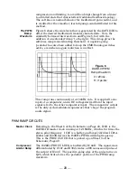
Figure 6 shows the waveform that is generated by the

DAVID-III

 to

affect the desired feedforward transfer characteristic.  Note the

similarity between this waveform and Figure 5, but with the

addition of an extended  droop  to the right.  This droop gives the

soft knee compression/limiting threshold.  A negative-going

pedestal  has also been added to keep the CMOS analog switches

active, even when no gain reduction is in effect.

Figure 6

DAVID-III

 PWM

Ramp Waveform

V=2V/div.
H=1µs/div.

This ramp runs continuously at a 152kHz rate.  It is applied to one

input of a comparator, and a DC voltage derived from the input

signal is fed to the other comparator input.  The comparator output

is the duty-cycle-modulated squarewave that  chops  the program

audio signal.

PWM RAMP CIRCUITS

Master Clock

Referring to the Sheet 6 of the Schematic on Page 43, IC3D is the

DAVID-III

 master clock running at 1.216MHz, which is 64 times the

stereo pilot frequency.  IC3C is a buffer, and binary dividers IC21A,

IC43A and IC43B derive the 152kHz PWM switching frequency.

This is the PROC CLOCK that is picked up on Sheet 3 of the

Schematic, Page 40.

Compressor/

Limiter Ramp

The 152kHz PROC CLOCK is buffered by IC44D.  The squarewave

differentiated by C107 and R302 creates a 200 nanosecond pulse at

the output of IC44C.  The positive-going edge of the pulse turns on

Q25, which brute-forces the  pedestal  portion of the PWM ramp

waveform.

Summary of Contents for DAVID-III 718

Page 1: ...OPERATING AND MAINTENANCE INSTRUCTION MANUAL DAVID III FM STEREO PROCESSOR GENERATOR MODEL 718 ...

Page 2: ......

Page 3: ...chased __________________ Warranty Card Mailed o OPERATING AND MAINTENANCE INSTRUCTION MANUAL DAVID III FM STEREO PROCESSOR GENERATOR June 2004 1305 Fair Avenue Santa Cruz CA 95060 TEL 831 458 0552 FAX 831 458 0554 Visit our Website www inovon com MODEL 718 ...

Page 4: ......

Page 5: ...GE SELECTION 8 Input Connections Unbalanced Inputs Input Grain Range Gain Jumpers PRE EMPHASIS SELECTION 9 COMPOSITE MPX OUTPUT 9 Section III SETUP AND OPERATION PANEL CONTROLS AND INDICATORS 10 NORMAL SETUP PROCEDURE 12 INPUT GAIN Calibration MPX LEVEL Adjustment TRIBAND PROCESSING SETUP GUIDELINES 14 AGC Section Notes MASTER DRIVE BASS and BRILLIANCE FINAL PEAK CONTROL 16 PIPP LIMITER COMP CLIPP...

Page 6: ...WM Comparators Gain Reduction Indicators Combining Amplifier THE PIPP LIMITER 27 LOW PASS FILTER 28 Filter Overshoots Overshoot Compensation The Low Pass Filter PILOT AND SUBCARRIER SYNTHESIS 29 Clock Pilot Generation Center Sampling Subcarrier Generation Composite Clipper Combining Amplifier Output Filter Output Phase and Equalization Trimmers POWER SUPPLY 31 YOUR NOTES AND DOODLES 31 Section V A...

Page 7: ...ionality to the modestly priced DAVID series along with a bigger bolder and brighter sound Wider AGC capture multiband processing equalization adjustments and a proprietary final limiting system make the DAVID III the rival of far more expensive alternatives Features Leading features of the DAVID III include Comprehensive PWM audio processing with gain riding AGC three bands of compression and lim...

Page 8: ...ee asym metrical frequency bands with secondary platform time constants to compress program dynamics with average value weighting Crossover frequencies at 100Hz and 4kHz See Figure 7 Page 24 Processing Control Master processing drive is adjust able between 0dB and more than 12dB equating to a corresponding reduction in program dynamics and apparent loudness increase Equalization Adjustment range r...

Page 9: ...5 BLOCK DIAGRAM Figure 1 below is a simplified Block Diagram of the DAVID III A full set of schematic diagrams appears in the Appendix Section V Figure 1 Block Diagram DAVID III Model 718 ...

Page 10: ...of the Warranty and provide a means of tracing lost or stolen gear but also the user will automatically receive specific SERVICE OR MODIFI CATION INSTRUCTIONS should the factory issue them MOUNTING Rack Requirement The DAVID III mounts in a standard 19 inch equipment rack and requires only 1 inches 1U of vertical rack space The use of plastic washers is recommended to protect the painted finish ar...

Page 11: ...sure to install the appropriate fuse listed on the rear panel You can remove the factory strikethrough with a carcinogenic solvent and then cross out the inappropriate marking with an indelible felt pen Power Cord The detachable IEC type power cord supplied with the encoder is fitted with a North American standard male plug The individual cord conductors may be color coded in either of two ways 1 ...

Page 12: ...in 3 Input Gain Range The DAVID III can accommodate line level program inputs with a nominal Zero VU level between 15dBu and 10dBu This 25dB range is divided into two more manageable overlapping gain ranges that are selected by a series of four internal jumpers As shipped the DAVID III is set up for professional level inputs that lie in the 0dBu to 10dBu range Most console and STL receiver outputs...

Page 13: ...nd both jumpers must be set identically as shown in Figure 3 below Jumpers for 75µs Jumpers for 50µs Figure 3 Pre Emphasis Jumpering COMPOSITE MPX OUTPUT The unbalanced COMPOSITE MPX OUT BNC connector on the rear panel of the DAVID III has a resistive source impedance of 75 ohms This allows cable runs of moderate length to about 50 feet to the exciter or microwave link input If the cable is more t...

Page 14: ...reo imbalance should be addressed at the source of this problem The INPUT GAIN control has a 12dB range which is extended by the input gain range jumpering options described on Page 8 INPUT GAIN is adjusted using normal program material to maintain the indicated AGC gain in the center of its operating region GATE OPEN DAVID III AGC is gated meaning that during brief pauses in the program the gain ...

Page 15: ...teristic The green 0dB indicator remains lighted at full brilliance with full gain no processing in the attendant band When the 12dB LED is lighted fully 12dB or more limiting and compression is in effect Equal brightness in both LEDs would suggest about 6dB of gain reduction With a little practice it should not be difficult to visually interpolate for intermediate G R values as well as to differe...

Page 16: ...ermediate STL or other link in either the input or the output path of the DAVID III may call for considerations not addressed here At this point the DAVID III should be installed in the program chain with power applied The MODE switch should be in STEREO and the PIPP LIMITER switched ON INPUT GAIN Calibration The single INPUT GAIN adjustment controls both stereo channels simultaneously It is set s...

Page 17: ...ction 7 OPTIONAL If an RDS or an SCA subcarrier is to be transmitted connect it to the proper combining point at this time Using the Mod Monitor or other means of reading the auxiliary subcarrier injection level adjust the subcarrier level control for the proper injection This is normally about 4 for an RDS subcarrier and 10 for an audio SCA 8 Put the Mod Monitor back into its Total Peak Modulatio...

Page 18: ...ould constitute a case of overprocessing of the musical content of the program The correction rate of the AGC stage has been speeded up from previous DAVID versions by a factor of four The present value is about 2dB second just a bit slower than would result in audible dynamic alteration of the program given the averaging response to music and speech MASTER DRIVE This sets the amount of overall pr...

Page 19: ...e same as the unprocessed program input though the program dynamic range will be restricted based on how MASTER DRIVE has been set Rotating BASS and BRILLIANCE toward 3dB will cause a reduction of energy at the ends of the spectrum The BASS control gives up to 9dB of low end Spectral Loading BRILLIANCE however affords only a maximum 6dB BRILLIANCE is purposely restricted because of FM broadcast sy...

Page 20: ...sound more saxophone like and speech will definitely have a different quality But after all we are talking audio processing here and sonic modification is par for the course Another possible concern might be that mucking about with waveform symmetry could introduce a sufficient DC component to the program that the exciter frequency reference PLL would unlock Take comfort in the fact that audio pro...

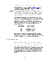
Page 21: ...he pilot frequency The following tabulation is an approximation of the SGTM Spectral Garbage generated by composite clipping COMPOSITE PROCESSING PEAK VALUE OF CLIPPING PRODUCTS OUT 60dB below 100 Mod 1dB 50dB below 100 Mod 2dB 45dB below 100 Mod 3dB 40dB below 100 Mod Keep clearly in mind that crosstalk of program audio harmonic components into the RDS or SCA subcarrier region is exacerbated by c...

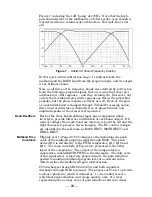
Page 22: ...roadcast audio processing was pioneered by Inovonics in the early 1980s and has been refined over the years PWM is a simple colorless quasi digital method of linear gain control that avoids several hassles associated with more expensive and possibly single sourced VCA integrated circuits Our implementation of PWM utilizes the popular 4000 series CMOS parts that are dirt cheap and available in any ...

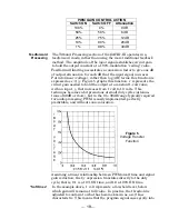
Page 23: ...d the output at a constant 1 volt value with an input y that increases from 1 volt to 10 volts This technique becomes a bit precarious at small duty cycles attenua tions of 40dB or more but in the 0 to 30dB range typically required for audio processing PWM is easily implemented perfectly predictable and without sonic coloration Figure 5 Voltage Transfer Function Assuming a linear relationship betw...

Page 24: ...Ramp Waveform V 2V div H 1µs div This ramp runs continuously at a 152kHz rate It is applied to one input of a comparator and a DC voltage derived from the input signal is fed to the other comparator input The comparator output is the duty cycle modulated squarewave that chops the program audio signal PWM RAMP CIRCUITS Master Clock Referring to the Sheet 6 of the Schematic on Page 43 IC3D is the DA...

Page 25: ...he AGC stage works in a feedback mode the R C ramp gives a constant dB per second control rate over the 30dB AGC range SIGNAL PATH CIRCUITRY NOTE Left and right program channel circuits are identical so only the left channel will be described in detail A skilled technical professional should be able to extrapolate the circuit descriptions for the right channel INPUT STAGES Line Input Balancing Lea...

Page 26: ...rging C97 through R298 and R299 When the program level is below the reference CR51 is reverse biased and C97 discharges through R299 and R297 Integration by R299 and C97 determine the AGC correction rate DC buffered by IC45D is presented to one input of a comparator comprised of Q27 Q28 and Q29 The AGC ramp is fed to the other comparator input and the output from Q29 is the PWM control for the fou...

Page 27: ...h program peaks are hard clipped The effect of clipping at this point is seldom ever audible In the first place sadly few CD music tracks contain peaks more than 10dB above the true average level of the music Secondly clipping is in the pre emphasized domain This means that clipping artifacts are attenuated by receiver de emphasis Finally the program derived DC value is a simple average and not ba...

Page 28: ...s a companion phase inverter to provide full wave rectification of each band output DC control voltages from each band are common to both the left and the right channels to preserve stereo imaging The DC control voltages are identified in the schematic as BASS RECT MSTR RECT and BRILL RECT Midband Time Constants Flipping over to Page 40 C55 charges to the instantaneous peak value of the midband pr...

Page 29: ... at 12 only the quiescent 10dB worth of gain spoiling from R174 is in effect and processing is at maximum so far as levels are concerned As MASTER DRIVE is turned further clockwise from 12 to MAX something else happens The wiper of R183 begins to go negative because of bias through R181 This has two effects First the quiescent gain spoiling voltage through R174 is reduced somewhat which has the ef...

Page 30: ...wn Brilliance Processing Because the brilliance band involves frequencies of 4kHz and up gain control action can afford to be very fast Attack is near instantaneous as C75 charges through R208 The integrated DC is applied directly to PWM comparator Q20 Q19 and Q18 Spectral Loading for the brilliance band is identical to that described above for the bass band The only difference is R214 inserted in...

Page 31: ...2B through R199 and R198 C68 and C69 turn this stage into a unity gain low pass filter The bases of Q11 and Q12 are connected to the junction of R199 and R198 The emitters of these transistors are clamped at DC levels representing the absolute output ceiling of the DAVID III Thus Q11 and Q12 will always serve as hard clippers for program peaks that exceed the assigned ceiling value But each of the...

Page 32: ... there is little tendency for the filter to generate overshoots Overshoot Compensation Thumbing to Page 42 IC31B includes a phase lag network that displaces the fast leading and trailing edges of steep waveforms in time This means that the primary time domain characteristic of a program waveform that would normally excite filter overshoots is instead added to the waveform amplitude CR29 and CR28 a...

Page 33: ...p down BCD counter clocked at the 608kHz sampling frequency 1 of 10 decoder IC9 OR gate IC8B and binary divider IC7A work together to keep IC10 continually counting from zero to 8 back down to zero etc Counting logic is decoded by a 1 of 9 de multiplexer IC18 and IC20A that samples a resistor string with sine weighted values This generates one half a sinewave for each counting cycle IC21B reverses...

Page 34: ...arrier generation and L R audio appears at the DAVID III output S2 also stops the stereo pilot in the MONO mode Composite Clipper Diodes CR12 and CR13 are biased to the same 100 modulation level established by the PIPP Limiter and overshoot compensation circuits The buffered composite signal less the stereo pilot is pre sented to this clipper through front panel COMP CLIPPING control R36 When R36 ...

Page 35: ...e stereo separation POWER SUPPLY DAVID III circuitry operates from the bipolar 9 volt supply diagrammed on Page 42 The two supplies are regulated by linear three terminal IC voltage regulators IC1 for the 9 volt supply IC2 for the 9 volt supply The power transformer has dual primary windings that may be switched in parallel or in series for 115V or 230V mains respectively YOUR NOTES AND DOODLES ar...

Page 36: ...32 ...

Page 37: ...33 Section V APPENDIX This section of the DAVID III Manual contains Parts Listings Schematic Diagrams and an explanation of Inovonics Generous and Liberal Warranty Policy ...

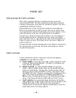
Page 38: ...d circuit board and those in the 600s are chassis mounted components PARTS LISTINGS Unless specifically noted by component reference designation capacitors are specified as follows a Under 100pF are general purpose disc ceramic capacitors with no specific technical specification The letter following the value indicates picofarads b 100pF to 0 47µF are of the metallized Mylar or polyester variety W...

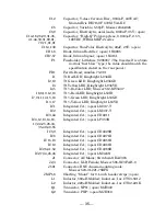
Page 39: ...934YD I4 5 T1 Bi Color LED Mouser 512 MV5437 I6 8 10 12 18 T1 Red LED Kingbright L53ID I7 9 11 14 15 16 T1 Green LED Kingbright L53GD I13 17 T1 Yellow LED Kingbright L53YD IC1 Integrated Cct open LM317 T IC2 Integrated Cct open LM337 T IC3 44 Integrated Cct open CD4011 IC4 12 13 14 16 17 22 25 28 33 35 40 48 55 Integrated Cct open LF353N IC5 9 Integrated Cct open CD4028B IC8 Integrated Cct open CD...

Page 40: ...10K Piher PT10MH01 103A2020 with Figure 15 spindle Inovonics P N 0580 S1 Switch Voltage Selector ITW 18 000 0022 S2 3 Switch SPDT Toggle C K 7101 M D9 A B E T1 Transformer Power Signal LP 20 600 or direct cross ref Y1 Crystal 1 216MHz Inovonics P N 1242 PARTS SUPPLIERS Inovonics strives to maintain factory stock of all parts used in the products we manufacture A large proportion of the components ...

Page 41: ...ny semiconductor IC capacitor resistor or connector used in the DAVID III will be available from one or more of these firms Each supplier maintains a Website and publishes a full line printed catalog which is free for the asking Minimum order restrictions may apply and export orders may prove somewhat problematical Mouser Electronics www mouser com 1 800 346 6873 Digi Key Corporation www digikey c...

Page 42: ...38 ...

Page 43: ...39 ...

Page 44: ...40 ...

Page 45: ...41 ...

Page 46: ...42 ...

Page 47: ...43 ...

Page 48: ...44 ...

Page 49: ...ion or if the serial identification label has been removed or altered III TERMS OF WARRANTY Inovonics Inc products are warranted to be free from defects in materials and workmanship A Any discrepancies noted within ONE YEAR of the date of delivery will be repaired free of charge or the equipment will be replaced with a new or remanufactured product at Inovonics option B Parts and labor for factory...

Reviews: