27
stages is such that the green LED glows at full brightness with no
reduction in effect, fading to full-brightness of the red LED with
12dB of reduction. Midway through the display range, both LEDs
should be lit about halfway.
Combining
Amplifier
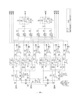
Back on Page 39, IC33B is a current-summing combining amplifier
and low-pass filter. The three frequency bands are summed through
resistors R235, R234 and R233, with a CMOS analog switch sections
in series with each.
Gain-control PWM drives the analog switches, the duty cycle
effectively multiplying the 3k series resistor. When the duty cycle is
50% in the bass band, R235 looks like 6k. At 10%, the effective
resistance is 30k. The current-summing configuration of IC33B
eliminates interaction between the bands, and the low-pass response
removes the 152kHz switching frequency.
THE PIPP* LIMITER
The operating theory of the PIPP* Limiter is detailed on Page 16.
Though the subject US Patent covers various analog and digital
implementations of the fundamental concept, the configuration used
in the
DAVID-III
is absurdly simple.
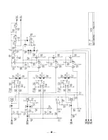
On Page 41, the program audio signal from the Triband Processor
section is routed to IC32B through R199 and R198. C68 and C69
turn this stage into a unity-gain low-pass filter.
The bases of Q11 and Q12 are connected to the junction of R199 and
R198. The emitters of these transistors are clamped at DC levels
representing the absolute output ceiling of the
DAVID-III
. Thus
Q11 and Q12 will always serve as hard clippers for program peaks
that exceed the assigned ceiling value. But each of these two
transistors is part of a voltage amplifier as well.
Using the Q12 side of the circuit for an illustration, as the program
signal approaches the final clipping point Q12 begins to conduct,
which turns on Q14 to begin charging C40. Voltage developed at the
top of C40 turns on Q5, which is connected to the program signal
path through R102 and CR18. As Q5 conducts, positive waveform
excursions are maintained at the clipping threshold, which becomes
the final-limiting point. This action describes a closed-loop,
feedback peak limiter for positive program peaks. CR18 ensures
that this part of the circuit has no effect over the negative-going
program components.
The emitter of Q5 is biased to a DC level that cancels the forward
drop of CR18 and the saturation voltage of Q5. A small amount of
program signal current is applied to the base of Q5 to linearize the
transistor s dynamic conduction resistance over the range of the
collector voltage swing.

